VOTING POWER100.00%
DOWNVOTE POWER100.00%
RESOURCE CREDITS100.00%
REPUTATION PROGRESS74.33%
Net Worth
0.016USD
STEEM
0.279STEEM
SBD
0.000SBD
Effective Power
3.396SP
├── Own SP
0.000SP
└── Incoming DelegationsDeleg
+3.396SP
Detailed Balance
| STEEM | ||
| balance | 0.224STEEM | STEEM |
| market_balance | 0.000STEEM | STEEM |
| savings_balance | 0.000STEEM | STEEM |
| reward_steem_balance | 0.055STEEM | STEEM |
| STEEM POWER | ||
| Own SP | 0.000SP | SP |
| Delegated Out | 0.000SP | SP |
| Delegation In | 3.396SP | SP |
| Effective Power | 3.396SP | SP |
| Reward SP (pending) | 0.061SP | SP |
| SBD | ||
| sbd_balance | 0.000SBD | SBD |
| sbd_conversions | 0.000SBD | SBD |
| sbd_market_balance | 0.000SBD | SBD |
| savings_sbd_balance | 0.000SBD | SBD |
| reward_sbd_balance | 0.000SBD | SBD |
{
  "balance": "0.224 STEEM",
  "savings_balance": "0.000 STEEM",
  "reward_steem_balance": "0.055 STEEM",
  "vesting_shares": "0.000000 VESTS",
  "delegated_vesting_shares": "0.000000 VESTS",
  "received_vesting_shares": "5522.714512 VESTS",
  "sbd_balance": "0.000 SBD",
  "savings_sbd_balance": "0.000 SBD",
  "reward_sbd_balance": "0.000 SBD",
  "conversions": []
}
Account Info
| name | teardownit |
| id | 1782985 |
| rank | 1,132,297 |
| reputation | 5613713826 |
| created | 2023-01-19T10:57:18 |
| recovery_account | steemcurator01 |
| proxy | None |
| post_count | 82 |
| comment_count | 0 |
| lifetime_vote_count | 0 |
| witnesses_voted_for | 0 |
| last_post | 2024-05-15T07:17:00 |
| last_root_post | 2024-05-15T07:17:00 |
| last_vote_time | 2023-03-02T11:08:06 |
| proxied_vsf_votes | 0, 0, 0, 0 |
| can_vote | 1 |
| voting_power | 0 |
| delayed_votes | 0 |
| balance | 0.224 STEEM |
| savings_balance | 0.000 STEEM |
| sbd_balance | 0.000 SBD |
| savings_sbd_balance | 0.000 SBD |
| vesting_shares | 0.000000 VESTS |
| delegated_vesting_shares | 0.000000 VESTS |
| received_vesting_shares | 5522.714512 VESTS |
| reward_vesting_balance | 107.934967 VESTS |
| vesting_balance | 0.000 STEEM |
| vesting_withdraw_rate | 0.000000 VESTS |
| next_vesting_withdrawal | 1969-12-31T23:59:59 |
| withdrawn | 0 |
| to_withdraw | 0 |
| withdraw_routes | 0 |
| savings_withdraw_requests | 0 |
| last_account_recovery | 1970-01-01T00:00:00 |
| reset_account | null |
| last_owner_update | 1970-01-01T00:00:00 |
| last_account_update | 1970-01-01T00:00:00 |
| mined | No |
| sbd_seconds | 0 |
| sbd_last_interest_payment | 1970-01-01T00:00:00 |
| savings_sbd_last_interest_payment | 1970-01-01T00:00:00 |
{
  "id": 1782985,
  "name": "teardownit",
  "owner": {
    "weight_threshold": 1,
    "account_auths": [],
    "key_auths": [
      [
        "STM4umsnYdafe3gGJDMZq2DYiNmbr21FdXKxVXgNeJDV199mvpEPe",
        1
      ]
    ]
  },
  "active": {
    "weight_threshold": 1,
    "account_auths": [],
    "key_auths": [
      [
        "STM4xk31Yt5z9rExdpzDvzg4aPAp4NotceGjqkHpKaRCRG3Luj5Fh",
        1
      ]
    ]
  },
  "posting": {
    "weight_threshold": 1,
    "account_auths": [],
    "key_auths": [
      [
        "STM84vRsQnVUcYm2vUCvw8jhFgtt5Muic2P1KS4eU45qXyU4DtnR9",
        1
      ]
    ]
  },
  "memo_key": "STM7YnEoqSkCcCzD7gLY2Zwf14LRQRztAcSUTUYiiF6CkgJ5QAY9h",
  "json_metadata": "{}",
  "posting_json_metadata": "",
  "proxy": "",
  "last_owner_update": "1970-01-01T00:00:00",
  "last_account_update": "1970-01-01T00:00:00",
  "created": "2023-01-19T10:57:18",
  "mined": false,
  "recovery_account": "steemcurator01",
  "last_account_recovery": "1970-01-01T00:00:00",
  "reset_account": "null",
  "comment_count": 0,
  "lifetime_vote_count": 0,
  "post_count": 82,
  "can_vote": true,
  "voting_manabar": {
    "current_mana": "5522714512",
    "last_update_time": 1758264954
  },
  "downvote_manabar": {
    "current_mana": 1380678628,
    "last_update_time": 1758264954
  },
  "voting_power": 0,
  "balance": "0.224 STEEM",
  "savings_balance": "0.000 STEEM",
  "sbd_balance": "0.000 SBD",
  "sbd_seconds": "0",
  "sbd_seconds_last_update": "1970-01-01T00:00:00",
  "sbd_last_interest_payment": "1970-01-01T00:00:00",
  "savings_sbd_balance": "0.000 SBD",
  "savings_sbd_seconds": "0",
  "savings_sbd_seconds_last_update": "1970-01-01T00:00:00",
  "savings_sbd_last_interest_payment": "1970-01-01T00:00:00",
  "savings_withdraw_requests": 0,
  "reward_sbd_balance": "0.000 SBD",
  "reward_steem_balance": "0.055 STEEM",
  "reward_vesting_balance": "107.934967 VESTS",
  "reward_vesting_steem": "0.061 STEEM",
  "vesting_shares": "0.000000 VESTS",
  "delegated_vesting_shares": "0.000000 VESTS",
  "received_vesting_shares": "5522.714512 VESTS",
  "vesting_withdraw_rate": "0.000000 VESTS",
  "next_vesting_withdrawal": "1969-12-31T23:59:59",
  "withdrawn": 0,
  "to_withdraw": 0,
  "withdraw_routes": 0,
  "curation_rewards": 0,
  "posting_rewards": 110,
  "proxied_vsf_votes": [
    0,
    0,
    0,
    0
  ],
  "witnesses_voted_for": 0,
  "last_post": "2024-05-15T07:17:00",
  "last_root_post": "2024-05-15T07:17:00",
  "last_vote_time": "2023-03-02T11:08:06",
  "post_bandwidth": 0,
  "pending_claimed_accounts": 0,
  "vesting_balance": "0.000 STEEM",
  "reputation": "5613713826",
  "transfer_history": [],
  "market_history": [],
  "post_history": [],
  "vote_history": [],
  "other_history": [],
  "witness_votes": [],
  "tags_usage": [],
  "guest_bloggers": [],
  "rank": 1132297
}
Withdraw Routes
| Incoming | Outgoing |
|---|---|
Empty | Empty |
{
  "incoming": [],
  "outgoing": []
}From Date
To Date
steemdelegated 3.396 SP to @teardownit2025/09/19 06:55:54
steemdelegated 3.396 SP to @teardownit
2025/09/19 06:55:54
| delegatee | teardownit |
| delegator | steem |
| vesting shares | 5522.714512 VESTS |
| Transaction Info | Block #99231097/Trx 277273e3f9f7e2644a4f353b298dd136cb822dea |
View Raw JSON Data
{
  "block": 99231097,
  "op": [
    "delegate_vesting_shares",
    {
      "delegatee": "teardownit",
      "delegator": "steem",
      "vesting_shares": "5522.714512 VESTS"
    }
  ],
  "op_in_trx": 0,
  "timestamp": "2025-09-19T06:55:54",
  "trx_id": "277273e3f9f7e2644a4f353b298dd136cb822dea",
  "trx_in_block": 1,
  "virtual_op": 0
}2024/10/18 15:09:00
2024/10/18 15:09:00
| author | teardownit |
| permlink | power-supply-characteristics-turns-the-ac-dc-power-supply-on-and-off-low-cost-parameter-measurement |
| voter | botsgeek |
| weight | 10000 (100.00%) |
| Transaction Info | Block #89589661/Trx 00579235486a9a5cd5bf4935cf95a4734904c2c5 |
View Raw JSON Data
{
  "block": 89589661,
  "op": [
    "vote",
    {
      "author": "teardownit",
      "permlink": "power-supply-characteristics-turns-the-ac-dc-power-supply-on-and-off-low-cost-parameter-measurement",
      "voter": "botsgeek",
      "weight": 10000
    }
  ],
  "op_in_trx": 0,
  "timestamp": "2024-10-18T15:09:00",
  "trx_id": "00579235486a9a5cd5bf4935cf95a4734904c2c5",
  "trx_in_block": 7,
  "virtual_op": 0
}steemdelegated 3.498 SP to @teardownit2024/08/14 08:57:06
steemdelegated 3.498 SP to @teardownit
2024/08/14 08:57:06
| delegatee | teardownit |
| delegator | steem |
| vesting shares | 5688.439404 VESTS |
| Transaction Info | Block #87717054/Trx 6144600a68f103d9db642c5dca91f7d7da7d015c |
View Raw JSON Data
{
  "block": 87717054,
  "op": [
    "delegate_vesting_shares",
    {
      "delegatee": "teardownit",
      "delegator": "steem",
      "vesting_shares": "5688.439404 VESTS"
    }
  ],
  "op_in_trx": 0,
  "timestamp": "2024-08-14T08:57:06",
  "trx_id": "6144600a68f103d9db642c5dca91f7d7da7d015c",
  "trx_in_block": 8,
  "virtual_op": 0
}steemdelegated 10.499 SP to @teardownit2024/08/06 03:23:42
steemdelegated 10.499 SP to @teardownit
2024/08/06 03:23:42
| delegatee | teardownit |
| delegator | steem |
| vesting shares | 17075.678695 VESTS |
| Transaction Info | Block #87480671/Trx 86455537f450db70b680443170e87e15c75125d5 |
View Raw JSON Data
{
  "block": 87480671,
  "op": [
    "delegate_vesting_shares",
    {
      "delegatee": "teardownit",
      "delegator": "steem",
      "vesting_shares": "17075.678695 VESTS"
    }
  ],
  "op_in_trx": 0,
  "timestamp": "2024-08-06T03:23:42",
  "trx_id": "86455537f450db70b680443170e87e15c75125d5",
  "trx_in_block": 5,
  "virtual_op": 0
}bluesnipersent 0.010 STEEM to @teardownit- "Hello. Good to see you on Steem. To maximize your rewards, publish your post also on Hive ( hive.blog ) and Blurt ( blurt.blog ) blockchains. Use upvu, jsup or ctime and get instant upvotes"2024/05/15 07:22:51
bluesnipersent 0.010 STEEM to @teardownit- "Hello. Good to see you on Steem. To maximize your rewards, publish your post also on Hive ( hive.blog ) and Blurt ( blurt.blog ) blockchains. Use upvu, jsup or ctime and get instant upvotes"
2024/05/15 07:22:51
| amount | 0.010 STEEM |
| from | bluesniper |
| memo | Hello. Good to see you on Steem. To maximize your rewards, publish your post also on Hive ( hive.blog ) and Blurt ( blurt.blog ) blockchains. Use upvu, jsup or ctime and get instant upvotes |
| to | teardownit |
| Transaction Info | Block #85106684/Trx 15d8996fdab674632bf115204ac02cffa9cfc8c6 |
View Raw JSON Data
{
  "block": 85106684,
  "op": [
    "transfer",
    {
      "amount": "0.010 STEEM",
      "from": "bluesniper",
      "memo": "Hello. Good to see you on Steem. To maximize your rewards, publish your post also on Hive ( hive.blog ) and Blurt ( blurt.blog ) blockchains. Use upvu, jsup or ctime and get instant upvotes",
      "to": "teardownit"
    }
  ],
  "op_in_trx": 0,
  "timestamp": "2024-05-15T07:22:51",
  "trx_id": "15d8996fdab674632bf115204ac02cffa9cfc8c6",
  "trx_in_block": 5,
  "virtual_op": 0
}2024/05/15 07:22:30
2024/05/15 07:22:30
| author | teardownit |
| permlink | search-for-intermittent-faults-and-pupin-coils-using-a-reflectometer |
| voter | bluesniper |
| weight | 10000 (100.00%) |
| Transaction Info | Block #85106678/Trx e5c83496c806732d919beddd3da502c38dc8f8b1 |
View Raw JSON Data
{
  "block": 85106678,
  "op": [
    "vote",
    {
      "author": "teardownit",
      "permlink": "search-for-intermittent-faults-and-pupin-coils-using-a-reflectometer",
      "voter": "bluesniper",
      "weight": 10000
    }
  ],
  "op_in_trx": 0,
  "timestamp": "2024-05-15T07:22:30",
  "trx_id": "e5c83496c806732d919beddd3da502c38dc8f8b1",
  "trx_in_block": 1,
  "virtual_op": 0
}teardownitpublished a new post: search-for-intermittent-faults-and-pupin-coils-using-a-reflectometer2024/05/15 07:17:00
teardownitpublished a new post: search-for-intermittent-faults-and-pupin-coils-using-a-reflectometer
2024/05/15 07:17:00
| author | teardownit |
| body | Intermittent faults ('floating' defects) are damages that manifest themselves periodically and are caused by poor-quality core connections or reduced insulation resistance. Customer complaints about short-term connection losses are evidence of defects of this kind. Such defects may appear due to mechanical damage to the cable (for example, in the event of vibration from heavy vehicles, rotary equipment, etc., nearby). Typically, when a technician encounters this type of damage, he has to wait patiently for it to manifest itself, hoping the effect will last long enough to determine its location. There is no guarantee that the damage will reveal itself while the technician is on duty. The use of reflectometers allows one to automate this process and maximize productivity. Some reflectometers have a special function for detecting intermittent faults. The device connected to the line accumulates all reflectograms over a certain period and displays them superimposed on each other. Where the reflectogram differs, the intermittent fault is located. Finding intermittent faults For example, consider the following situation: a particular pair of cables works fine for the better part of the day, but there is a momentary failure out of the blue. 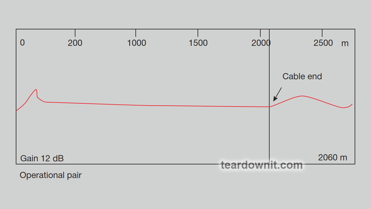 We get two reflectograms for the same pair (with different gain settings) when checked. In the first one, with a gain of 12 dB, a surge of positive polarity is observed on the reflectogram of a working pair at a distance of 6760 feet, corresponding to the end of the cable. In the second one, when the gain increases by 14 dB, an additional spike appears on the reflectogram, the nature of which indicates the presence of a coupling in the cable at a distance of 3280 feet. By further increasing the vertical gain level, the reflectogram will not reveal the slightest sign of damage along the entire length of the cable being tested. 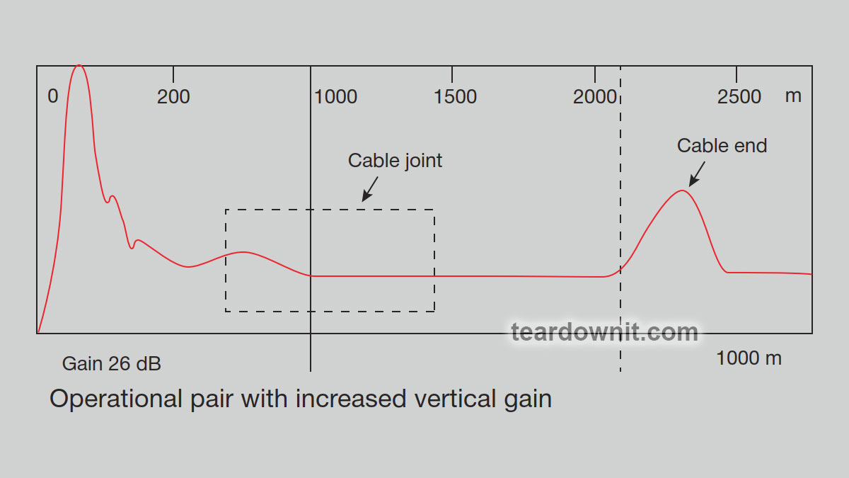 We will need the 'intermittent fault detection' function mentioned above. By continuously monitoring the pair's condition, the OTDR shows any deviations from the cable's rated impedance, allowing the location of intermittent faults to be pinpointed. The reflectometer display will show the current reflectograms obtained during testing. Periodic inspections allow one to determine whether signs of malfunction have appeared. Once the non-persistent damage has been captured, the result should look approximately as shown in the figure. The differences will be evident if one compares it with the previous one. A noticeable drop appears where there was nothing before. The location of the fault can be determined by simply moving the cursor to the front of the pulse reflected from the break and reading the distance from the display. Random vibrations or other irregular events cause the connections to loosen and electrical contact to be temporarily lost, resulting in a fault similar to a partial break. Note that at the moment this fault occurs, the pulse reflected from the far open end of the line decreases because, due to a poor connection in the cable coupling, the magnitude of the electrical signal reaching the end of the cable is reduced. What conclusions can be drawn? Almost every type of cable system is susceptible to intermittent faults. Such damage creates severe problems for users and technicians. The intermittent fault detection mode of reflectometers allows one to continuously monitor the cable over a long period, so the technician does not have to waste working hours waiting for the damage to manifest itself. Pupin coils Pupin coils can still be found on an analog telephone line. Pupin coils disrupt the homogeneity of the copper pair, turning it into an ideal low-pass filter with more substantial high-frequency attenuation. Therefore, a prerequisite for using any xDSL technologies on existing phone lines is the removal of Pupin coils, which have been found to have extensive applications in US telephone networks. Servicing xDSL systems can always result in such a problem. In this case, one will need a reflectometer with a function for searching and counting Pupin coils. Searching for installation locations of Pupin coils A reflectometer is the only device that allows one to simply and accurately determine the location of Pupin coils. Since the pulses sent by the reflectometer are high-frequency, they are reflected from the Pupin coil, a low-pass filter. The coil on the reflectogram looks like a significant increase in the cable impedance, i.e., similar to the reflectogram of a line break. 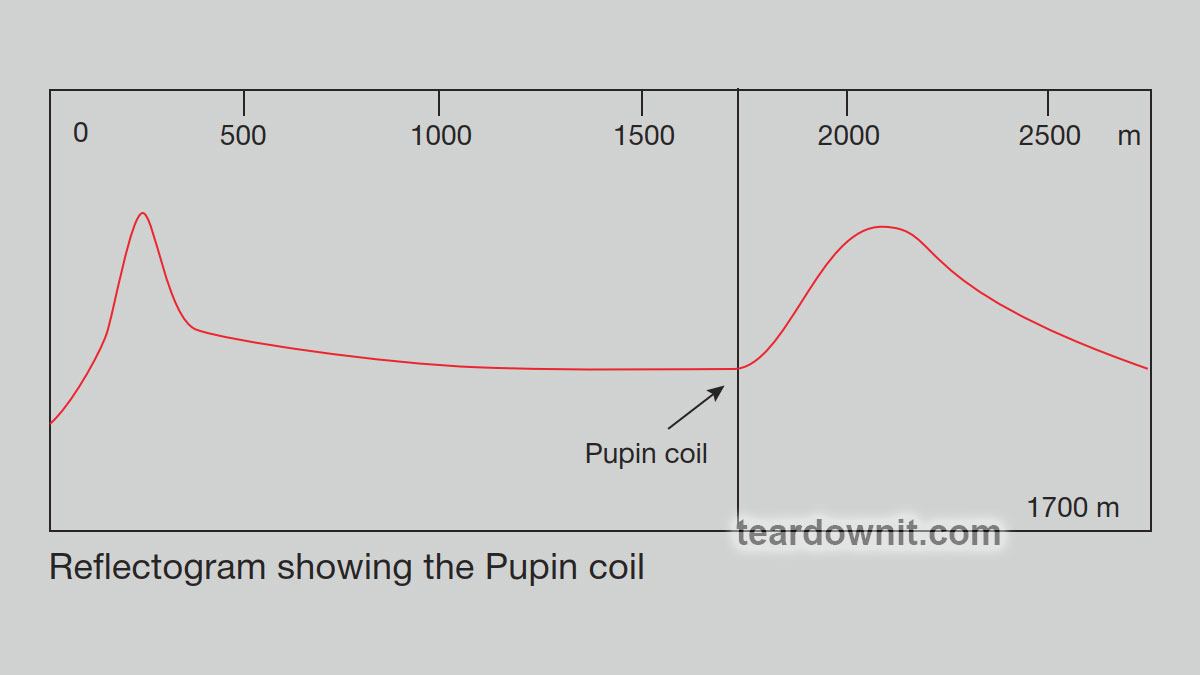 As you can see, the outline of the pulse reflected from the Pupin coil is more rounded than the pulse reflected from the cable brake, and the coil itself is located at a distance of about 5600 feet. In Eastern Europe, there are several Pupinization systems: medium, light, extra light, and broadcasting light. All systems have the same pitch of 1.7 km and differ in the inductance of the coils, the bandwidth of the transmitted frequencies, and the distance between the amplifiers. Unfortunately, the reflectogram shows only the first coil. |
| json metadata | {"tags":["aroundcable"],"image":["https://cdn.steemitimages.com/DQmZw1DmQFffYXc6vRy3XNdef56GdZfVjVfPN9aWYT2v4XZ/image.png","https://cdn.steemitimages.com/DQmT2vBPgJeK1mmNhfXcSp4n6NNJE8BUAYrGTs3xmmC3woF/image.png","https://cdn.steemitimages.com/DQmZXF7zmJqsiekyEwFZW8PsRTKjb2wvy5XzPn9M99u6Y2u/image.png"],"app":"steemit/0.2","format":"markdown"} |
| parent author | |
| parent permlink | aroundcable |
| permlink | search-for-intermittent-faults-and-pupin-coils-using-a-reflectometer |
| title | Search for intermittent faults, and Pupin coils using a reflectometer. |
| Transaction Info | Block #85106574/Trx a89287062fa9bb72bac32e030b6893b758c722de |
View Raw JSON Data
{
"block": 85106574,
"op": [
"comment",
{
"author": "teardownit",
"body": "Intermittent faults ('floating' defects) are damages that manifest themselves periodically and are caused by poor-quality core connections or reduced insulation resistance. Customer complaints about short-term connection losses are evidence of defects of this kind. Such defects may appear due to mechanical damage to the cable (for example, in the event of vibration from heavy vehicles, rotary equipment, etc., nearby).\n\nTypically, when a technician encounters this type of damage, he has to wait patiently for it to manifest itself, hoping the effect will last long enough to determine its location. There is no guarantee that the damage will reveal itself while the technician is on duty. The use of reflectometers allows one to automate this process and maximize productivity.\n\nSome reflectometers have a special function for detecting intermittent faults. The device connected to the line accumulates all reflectograms over a certain period and displays them superimposed on each other. Where the reflectogram differs, the intermittent fault is located.\n\nFinding intermittent faults\nFor example, consider the following situation: a particular pair of cables works fine for the better part of the day, but there is a momentary failure out of the blue.\n\n\n\nWe get two reflectograms for the same pair (with different gain settings) when checked. In the first one, with a gain of 12 dB, a surge of positive polarity is observed on the reflectogram of a working pair at a distance of 6760 feet, corresponding to the end of the cable. In the second one, when the gain increases by 14 dB, an additional spike appears on the reflectogram, the nature of which indicates the presence of a coupling in the cable at a distance of 3280 feet. By further increasing the vertical gain level, the reflectogram will not reveal the slightest sign of damage along the entire length of the cable being tested.\n\n\n\nWe will need the 'intermittent fault detection' function mentioned above. By continuously monitoring the pair's condition, the OTDR shows any deviations from the cable's rated impedance, allowing the location of intermittent faults to be pinpointed.\n\nThe reflectometer display will show the current reflectograms obtained during testing. Periodic inspections allow one to determine whether signs of malfunction have appeared. Once the non-persistent damage has been captured, the result should look approximately as shown in the figure.\n\nThe differences will be evident if one compares it with the previous one. A noticeable drop appears where there was nothing before. The location of the fault can be determined by simply moving the cursor to the front of the pulse reflected from the break and reading the distance from the display.\n\nRandom vibrations or other irregular events cause the connections to loosen and electrical contact to be temporarily lost, resulting in a fault similar to a partial break. Note that at the moment this fault occurs, the pulse reflected from the far open end of the line decreases because, due to a poor connection in the cable coupling, the magnitude of the electrical signal reaching the end of the cable is reduced.\n\nWhat conclusions can be drawn? Almost every type of cable system is susceptible to intermittent faults. Such damage creates severe problems for users and technicians. The intermittent fault detection mode of reflectometers allows one to continuously monitor the cable over a long period, so the technician does not have to waste working hours waiting for the damage to manifest itself.\n\nPupin coils\nPupin coils can still be found on an analog telephone line. Pupin coils disrupt the homogeneity of the copper pair, turning it into an ideal low-pass filter with more substantial high-frequency attenuation.\n\nTherefore, a prerequisite for using any xDSL technologies on existing phone lines is the removal of Pupin coils, which have been found to have extensive applications in US telephone networks. Servicing xDSL systems can always result in such a problem. In this case, one will need a reflectometer with a function for searching and counting Pupin coils.\n\nSearching for installation locations of Pupin coils\nA reflectometer is the only device that allows one to simply and accurately determine the location of Pupin coils. Since the pulses sent by the reflectometer are high-frequency, they are reflected from the Pupin coil, a low-pass filter. The coil on the reflectogram looks like a significant increase in the cable impedance, i.e., similar to the reflectogram of a line break.\n\n\n\nAs you can see, the outline of the pulse reflected from the Pupin coil is more rounded than the pulse reflected from the cable brake, and the coil itself is located at a distance of about 5600 feet. In Eastern Europe, there are several Pupinization systems: medium, light, extra light, and broadcasting light. All systems have the same pitch of 1.7 km and differ in the inductance of the coils, the bandwidth of the transmitted frequencies, and the distance between the amplifiers. Unfortunately, the reflectogram shows only the first coil.",
"json_metadata": "{\"tags\":[\"aroundcable\"],\"image\":[\"https://cdn.steemitimages.com/DQmZw1DmQFffYXc6vRy3XNdef56GdZfVjVfPN9aWYT2v4XZ/image.png\",\"https://cdn.steemitimages.com/DQmT2vBPgJeK1mmNhfXcSp4n6NNJE8BUAYrGTs3xmmC3woF/image.png\",\"https://cdn.steemitimages.com/DQmZXF7zmJqsiekyEwFZW8PsRTKjb2wvy5XzPn9M99u6Y2u/image.png\"],\"app\":\"steemit/0.2\",\"format\":\"markdown\"}",
"parent_author": "",
"parent_permlink": "aroundcable",
"permlink": "search-for-intermittent-faults-and-pupin-coils-using-a-reflectometer",
"title": "Search for intermittent faults, and Pupin coils using a reflectometer."
}
],
"op_in_trx": 0,
"timestamp": "2024-05-15T07:17:00",
"trx_id": "a89287062fa9bb72bac32e030b6893b758c722de",
"trx_in_block": 8,
"virtual_op": 0
}bluesnipersent 0.010 STEEM to @teardownit- "Hello. Good to see you on Steem. To maximize your rewards, publish your post also on Hive ( hive.blog ) and Blurt ( blurt.blog ) blockchains. Use upvu, jsup or ctime and get instant upvotes"2024/05/10 06:49:36
bluesnipersent 0.010 STEEM to @teardownit- "Hello. Good to see you on Steem. To maximize your rewards, publish your post also on Hive ( hive.blog ) and Blurt ( blurt.blog ) blockchains. Use upvu, jsup or ctime and get instant upvotes"
2024/05/10 06:49:36
| amount | 0.010 STEEM |
| from | bluesniper |
| memo | Hello. Good to see you on Steem. To maximize your rewards, publish your post also on Hive ( hive.blog ) and Blurt ( blurt.blog ) blockchains. Use upvu, jsup or ctime and get instant upvotes |
| to | teardownit |
| Transaction Info | Block #84962704/Trx 62ef5243c7b81a7ed9e469db1cca7dcc485596bc |
View Raw JSON Data
{
  "block": 84962704,
  "op": [
    "transfer",
    {
      "amount": "0.010 STEEM",
      "from": "bluesniper",
      "memo": "Hello. Good to see you on Steem. To maximize your rewards, publish your post also on Hive ( hive.blog ) and Blurt ( blurt.blog ) blockchains. Use upvu, jsup or ctime and get instant upvotes",
      "to": "teardownit"
    }
  ],
  "op_in_trx": 0,
  "timestamp": "2024-05-10T06:49:36",
  "trx_id": "62ef5243c7b81a7ed9e469db1cca7dcc485596bc",
  "trx_in_block": 0,
  "virtual_op": 0
}bluesniperupvoted (100.00%) @teardownit / how-does-binary-logic-work-shift-registers2024/05/10 06:49:12
bluesniperupvoted (100.00%) @teardownit / how-does-binary-logic-work-shift-registers
2024/05/10 06:49:12
| author | teardownit |
| permlink | how-does-binary-logic-work-shift-registers |
| voter | bluesniper |
| weight | 10000 (100.00%) |
| Transaction Info | Block #84962696/Trx ae6648d49adbd72c8c3476683dcf4bb7cd376322 |
View Raw JSON Data
{
  "block": 84962696,
  "op": [
    "vote",
    {
      "author": "teardownit",
      "permlink": "how-does-binary-logic-work-shift-registers",
      "voter": "bluesniper",
      "weight": 10000
    }
  ],
  "op_in_trx": 0,
  "timestamp": "2024-05-10T06:49:12",
  "trx_id": "ae6648d49adbd72c8c3476683dcf4bb7cd376322",
  "trx_in_block": 5,
  "virtual_op": 0
}teardownitpublished a new post: how-does-binary-logic-work-shift-registers2024/05/10 06:43:42
teardownitpublished a new post: how-does-binary-logic-work-shift-registers
2024/05/10 06:43:42
| author | teardownit |
| body |  Sometimes, a microcontroller does not have enough pins to receive signals from buttons or display them on LED indicators, control relays, etc. Sometimes, one needs to interconnect two digital devices with a single cable, and it would be great to transmit eight, sixteen, or more signals over two to three wires to avoid needing a thick cable. Or, let's say we just want to make a lighting effect for a street sign. One does not need a whole computer or a microcontroller for this task. All these cases (and many others) should be designed with shift registers.  As children, many of us had an NES (Nintendo Entertainment System) game console. Its gamepad had 8 buttons: a plus-shaped button for left, right, up, and down, then Select, Start, A, and B. And there were only five wires in the gamepad cable: ground, +5-volt power, and three signal wires. Meaning the state of eight buttons was transmitted over three wires. 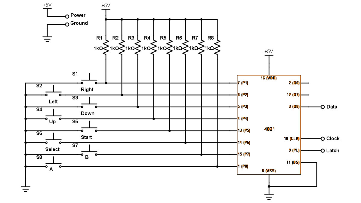 In the core of the gamepad is a single CD4021 chip. It is an 8-stage parallel input/serial output shift register. Here is a diagram of its internal logic: the chip has eight inputs for parallel input and outputs from the last three flip-flops. 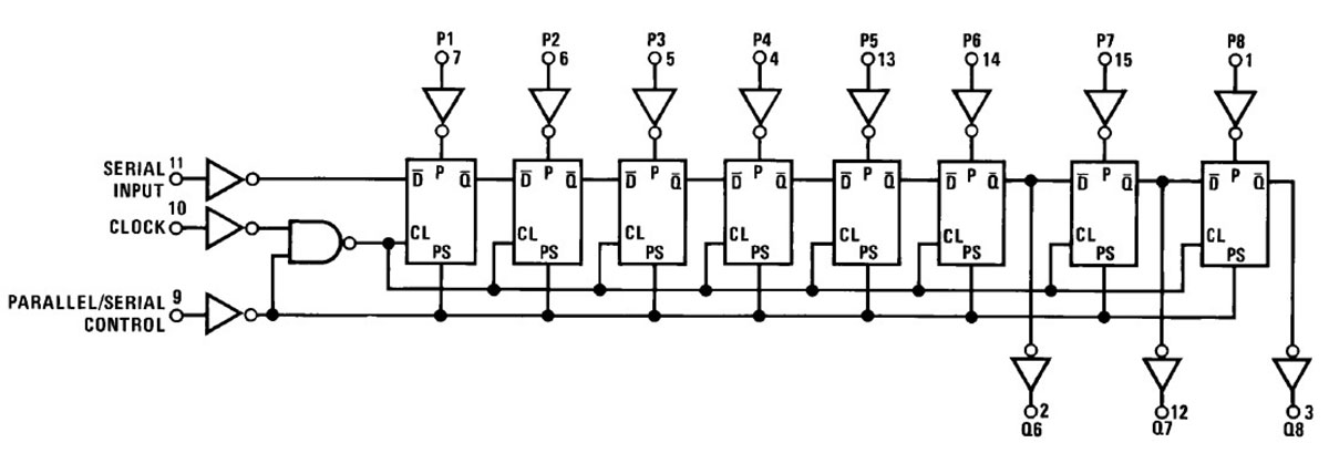 This should look familiar to our audience: a sequence of synchronous D flip-flops passing the torch of data bits from one to another. Oh, that's our combination lock from the post on flip-flops!  The CD4021 chip has two operating modes: serial and parallel. In parallel mode, eight flip-flops store information from eight inputs, each individually, regardless of clock pulses.  In serial mode, at the edge of the clock pulse, each subsequent flip-flop receives a data bit from the previous one, and the first flip-flop gets an incoming one from the serial input. Then, where is the input pin to reset all flip-flops? The answer is there's none. However, you can pull the serial input low and send eight consecutive clock pulses. If necessary, we can write zeros to all memory cells. Although, in the case of a gamepad, one can do without it. Simply switch the chip to parallel input mode, and it will save the state of the buttons. Pressed-down buttons correspond to logical zeros; released buttons correspond to logical ones because parallel inputs of the CD4021 in the NES gamepad are pulled by resistors to the power supply positive.  In this case, the DATA wire connected to the output of the eighth flip-flop will contain the state of the button S8 ('A'). We switch the chip to serial mode, apply clock pulses, and read S7 ('B'), then S6 ('Select'), all the way to S1 ('Right'). Congratulations! We have read the state of eight buttons via three signal wires (plus two power wires). Then we toggle to parallel mode again, rinse and repeat. This mode toggling is performed lightning fast, and the player will feel like the console responds to button presses instantly. But what if it’s the other way around, and one doesn’t need to read information from buttons but to write it into cells, for example, by lighting LEDs? Then, a shift register with serial input and parallel output will help. An example of such a shift register is CD40194. Unlike CD4021, it has not 8, but only 4 digits. Yet it's got parallel output and input, as well as serial input, with the ability to shift both to the right and left!  Does the CD40194 have a serial output, though? I hear you asking. Of course, it has! Q3 will be the serial output when shifted to the right, and Q0 will be the serial output when shifted to the left. The CD40194 also has a general reset input. And there are also two mode selection inputs: S0 and S1.  When S0 = 0 and S1 = 0, nothing happens. The chip does not respond to signals other than a general reset, retaining the saved 4 bits of information present at its outputs Q0..Q3. When S0 = 1 and S1 = 0, a shift to the right occurs at the leading edge of the clock pulse, from Q0 towards Q3. And the value from the left-most serial input is written to Q0. When S0 = 0 and S1 = 1, a shift to the left occurs at the leading edge of the clock pulse, from Q3 towards Q0. Q3 records the logic level from the right-most serial input. When S0 = 1 and S1 = 1, logic levels from parallel inputs are read and passed to the output. Moreover, unlike the CD4021, this action requires the leading edge of the clock pulse! A low level on the master reset input sets all outputs to zero, regardless of clock pulses and the selected operating mode. Let's assemble a simple experimental setup to get a complete picture of the CD40194 chip's operation. According to the most common scheme, the clock generator is assembled on the U4 NE555 chip. Pulses from its output are sent to the input of CLK U3 CD40194.  Using the SW2 block of 4 microswitches, you can send logical ones and zeros to the parallel inputs of the shift register. Resistors of the set RN1 pull the inputs high, and closed switches connect them to the ground, i.e., pull them low to obtain logical zero. The reset button SW3 with the pull-up resistor R3 works the same way. The U1 chip is a four-ship of double-input NAND gates. Both inputs of elements U1C and U1D are connected to each other. This way, the NAND element loses 'AND' and turns into the 'N' (NOT) element—a logical inverter. Through the inverter U1C, the inverted signal from the left-most output of Q0 goes to the left-shift input, and through U1D, the inverted logic level from the right-most output of Q3 goes to the right-shift input. Thus, when switching the mode to shift-right, the inverted value of Q3 will be written to Q0; the previous value of Q0 moves to Q1, previous Q1 to Q2, and previous Q2 to Q3. If the initial state before switching to right shift was all zeros, or if you keep pressing reset in right-shift mode, the register will gradually fill with ones. When the flow of ones reaches the end (Q3), the value one will be inverted, and the register will start filling itself with zeros. And when a zero reaches Q3, the cycle will repeat. The same process will only happen in the opposite direction when switching to the shift left mode. And in parallel input mode, the register will read the position of the microswitches whenever a clock pulse arrives. To visually indicate the operating modes of the CD40194 shift register, we've assembled a two-digit pulse counter on two flip-flops of the U2 CD4027. They operate as a frequency divider and cycle between four states: 00 → 01 → 10 → 11. The state of the CD40194's outputs is indicated by four red LEDs. The status of its control inputs is indicated by two blue LEDs (one of which had to be replaced with a green one because the blue one was faulty). The LEDs are turned on using S9014 transistors. Pulses for a two-bit binary counter that switches shift register modes are generated by an RS flip-flop on two NAND gates, U1A and U2A. It switches when the button SW1 is pressed. We've talked about the operation of such a circuit in the post about flip-flops. The video shows this experimental circuit board in operation. https://youtu.be/paNMGlQdO5A |
| json metadata | {"tags":["diyelectronics"],"image":["https://cdn.steemitimages.com/DQmXkiMtMLb2XaniYwgS7kp7SHyjhf9kTM3v6h46FJ5eo5H/image.png","https://cdn.steemitimages.com/DQmTA6K8RbYWv6hdYMNGhs1yaKenz6nk7PSzRsY6KsxMBGq/image.png","https://cdn.steemitimages.com/DQmRGsJvcEi8G2VvUMqNMjg2SGedCJmSj7UJcL9oLnHwG2i/image.png","https://cdn.steemitimages.com/DQmchQCAhwMEGMCNt9nP4eUE1GvvLXVFkCVaguBcoeEuidH/image.png","https://cdn.steemitimages.com/DQmW6X4SvoVeukeq2mH4hsB8RA1gVRKQ3sRNC6YX9b4pcgp/image.png","https://cdn.steemitimages.com/DQmTS7vFxdaZ9ePZoMEgH8byaczHk5MpD1VkmoPFDPhhVoi/image.png","https://cdn.steemitimages.com/DQmTpatdzeXMZiqxpsSdWJQPBTqFb3h6oCH8rknTnTLyjsV/image.png","https://cdn.steemitimages.com/DQmTv7q8o7H8YRG4eq4YWaqB7WQ7QN4nkCz9m2SN2DFCPTv/image.png","https://cdn.steemitimages.com/DQmZNDgF5dsus8TtMMD7GuTFkGJycfAq5BYEvReX7awzBmv/image.png","https://img.youtube.com/vi/paNMGlQdO5A/0.jpg"],"links":["https://youtu.be/paNMGlQdO5A"],"app":"steemit/0.2","format":"markdown"} |
| parent author | |
| parent permlink | diyelectronics |
| permlink | how-does-binary-logic-work-shift-registers |
| title | How does binary logic work? Shift registers |
| Transaction Info | Block #84962586/Trx a50f4df1731c84c5c43d0a1e0ca345ce8b49efec |
View Raw JSON Data
{
"block": 84962586,
"op": [
"comment",
{
"author": "teardownit",
"body": "\n\nSometimes, a microcontroller does not have enough pins to receive signals from buttons or display them on LED indicators, control relays, etc.\n\nSometimes, one needs to interconnect two digital devices with a single cable, and it would be great to transmit eight, sixteen, or more signals over two to three wires to avoid needing a thick cable.\n\nOr, let's say we just want to make a lighting effect for a street sign. One does not need a whole computer or a microcontroller for this task. All these cases (and many others) should be designed with shift registers.\n\n\n\nAs children, many of us had an NES (Nintendo Entertainment System) game console. Its gamepad had 8 buttons: a plus-shaped button for left, right, up, and down, then Select, Start, A, and B. And there were only five wires in the gamepad cable: ground, +5-volt power, and three signal wires. Meaning the state of eight buttons was transmitted over three wires.\n\n\n\nIn the core of the gamepad is a single CD4021 chip. It is an 8-stage parallel input/serial output shift register. Here is a diagram of its internal logic: the chip has eight inputs for parallel input and outputs from the last three flip-flops.\n\n\n\nThis should look familiar to our audience: a sequence of synchronous D flip-flops passing the torch of data bits from one to another. Oh, that's our combination lock from the post on flip-flops!\n\n\n\nThe CD4021 chip has two operating modes: serial and parallel. In parallel mode, eight flip-flops store information from eight inputs, each individually, regardless of clock pulses.\n\n\n\nIn serial mode, at the edge of the clock pulse, each subsequent flip-flop receives a data bit from the previous one, and the first flip-flop gets an incoming one from the serial input.\n\nThen, where is the input pin to reset all flip-flops? The answer is there's none. However, you can pull the serial input low and send eight consecutive clock pulses. If necessary, we can write zeros to all memory cells. Although, in the case of a gamepad, one can do without it.\n\nSimply switch the chip to parallel input mode, and it will save the state of the buttons. Pressed-down buttons correspond to logical zeros; released buttons correspond to logical ones because parallel inputs of the CD4021 in the NES gamepad are pulled by resistors to the power supply positive.\n\n\n\nIn this case, the DATA wire connected to the output of the eighth flip-flop will contain the state of the button S8 ('A'). We switch the chip to serial mode, apply clock pulses, and read S7 ('B'), then S6 ('Select'), all the way to S1 ('Right').\n\nCongratulations! We have read the state of eight buttons via three signal wires (plus two power wires). Then we toggle to parallel mode again, rinse and repeat. This mode toggling is performed lightning fast, and the player will feel like the console responds to button presses instantly.\n\nBut what if it’s the other way around, and one doesn’t need to read information from buttons but to write it into cells, for example, by lighting LEDs? Then, a shift register with serial input and parallel output will help.\n\nAn example of such a shift register is CD40194. Unlike CD4021, it has not 8, but only 4 digits. Yet it's got parallel output and input, as well as serial input, with the ability to shift both to the right and left!\n\n\n\nDoes the CD40194 have a serial output, though? I hear you asking. Of course, it has! Q3 will be the serial output when shifted to the right, and Q0 will be the serial output when shifted to the left.\n\nThe CD40194 also has a general reset input. And there are also two mode selection inputs: S0 and S1.\n\n\n\n\nWhen S0 = 0 and S1 = 0, nothing happens. The chip does not respond to signals other than a general reset, retaining the saved 4 bits of information present at its outputs Q0..Q3.\n\nWhen S0 = 1 and S1 = 0, a shift to the right occurs at the leading edge of the clock pulse, from Q0 towards Q3. And the value from the left-most serial input is written to Q0.\n\nWhen S0 = 0 and S1 = 1, a shift to the left occurs at the leading edge of the clock pulse, from Q3 towards Q0. Q3 records the logic level from the right-most serial input.\n\nWhen S0 = 1 and S1 = 1, logic levels from parallel inputs are read and passed to the output. Moreover, unlike the CD4021, this action requires the leading edge of the clock pulse!\n\nA low level on the master reset input sets all outputs to zero, regardless of clock pulses and the selected operating mode.\n \nLet's assemble a simple experimental setup to get a complete picture of the CD40194 chip's operation.\n\nAccording to the most common scheme, the clock generator is assembled on the U4 NE555 chip. Pulses from its output are sent to the input of CLK U3 CD40194.\n\n\n\n\nUsing the SW2 block of 4 microswitches, you can send logical ones and zeros to the parallel inputs of the shift register. Resistors of the set RN1 pull the inputs high, and closed switches connect them to the ground, i.e., pull them low to obtain logical zero.\n\nThe reset button SW3 with the pull-up resistor R3 works the same way.\n\nThe U1 chip is a four-ship of double-input NAND gates. Both inputs of elements U1C and U1D are connected to each other. This way, the NAND element loses 'AND' and turns into the 'N' (NOT) element—a logical inverter.\n\nThrough the inverter U1C, the inverted signal from the left-most output of Q0 goes to the left-shift input, and through U1D, the inverted logic level from the right-most output of Q3 goes to the right-shift input.\n\nThus, when switching the mode to shift-right, the inverted value of Q3 will be written to Q0; the previous value of Q0 moves to Q1, previous Q1 to Q2, and previous Q2 to Q3.\n\nIf the initial state before switching to right shift was all zeros, or if you keep pressing reset in right-shift mode, the register will gradually fill with ones.\n\nWhen the flow of ones reaches the end (Q3), the value one will be inverted, and the register will start filling itself with zeros. And when a zero reaches Q3, the cycle will repeat.\n\nThe same process will only happen in the opposite direction when switching to the shift left mode.\n\nAnd in parallel input mode, the register will read the position of the microswitches whenever a clock pulse arrives.\n\nTo visually indicate the operating modes of the CD40194 shift register, we've assembled a two-digit pulse counter on two flip-flops of the U2 CD4027. They operate as a frequency divider and cycle between four states: 00 → 01 → 10 → 11.\n\nThe state of the CD40194's outputs is indicated by four red LEDs. The status of its control inputs is indicated by two blue LEDs (one of which had to be replaced with a green one because the blue one was faulty). The LEDs are turned on using S9014 transistors.\n\nPulses for a two-bit binary counter that switches shift register modes are generated by an RS flip-flop on two NAND gates, U1A and U2A. It switches when the button SW1 is pressed. We've talked about the operation of such a circuit in the post about flip-flops.\n\nThe video shows this experimental circuit board in operation.\n\nhttps://youtu.be/paNMGlQdO5A",
"json_metadata": "{\"tags\":[\"diyelectronics\"],\"image\":[\"https://cdn.steemitimages.com/DQmXkiMtMLb2XaniYwgS7kp7SHyjhf9kTM3v6h46FJ5eo5H/image.png\",\"https://cdn.steemitimages.com/DQmTA6K8RbYWv6hdYMNGhs1yaKenz6nk7PSzRsY6KsxMBGq/image.png\",\"https://cdn.steemitimages.com/DQmRGsJvcEi8G2VvUMqNMjg2SGedCJmSj7UJcL9oLnHwG2i/image.png\",\"https://cdn.steemitimages.com/DQmchQCAhwMEGMCNt9nP4eUE1GvvLXVFkCVaguBcoeEuidH/image.png\",\"https://cdn.steemitimages.com/DQmW6X4SvoVeukeq2mH4hsB8RA1gVRKQ3sRNC6YX9b4pcgp/image.png\",\"https://cdn.steemitimages.com/DQmTS7vFxdaZ9ePZoMEgH8byaczHk5MpD1VkmoPFDPhhVoi/image.png\",\"https://cdn.steemitimages.com/DQmTpatdzeXMZiqxpsSdWJQPBTqFb3h6oCH8rknTnTLyjsV/image.png\",\"https://cdn.steemitimages.com/DQmTv7q8o7H8YRG4eq4YWaqB7WQ7QN4nkCz9m2SN2DFCPTv/image.png\",\"https://cdn.steemitimages.com/DQmZNDgF5dsus8TtMMD7GuTFkGJycfAq5BYEvReX7awzBmv/image.png\",\"https://img.youtube.com/vi/paNMGlQdO5A/0.jpg\"],\"links\":[\"https://youtu.be/paNMGlQdO5A\"],\"app\":\"steemit/0.2\",\"format\":\"markdown\"}",
"parent_author": "",
"parent_permlink": "diyelectronics",
"permlink": "how-does-binary-logic-work-shift-registers",
"title": "How does binary logic work? Shift registers"
}
],
"op_in_trx": 0,
"timestamp": "2024-05-10T06:43:42",
"trx_id": "a50f4df1731c84c5c43d0a1e0ca345ce8b49efec",
"trx_in_block": 7,
"virtual_op": 0
}bluesnipersent 0.010 STEEM to @teardownit- "Hello. Good to see you on Steem. To maximize your rewards, publish your post also on Hive ( hive.blog ) and Blurt ( blurt.blog ) blockchains. Use upvu, jsup or ctime and get instant upvotes"2024/04/29 06:43:21
bluesnipersent 0.010 STEEM to @teardownit- "Hello. Good to see you on Steem. To maximize your rewards, publish your post also on Hive ( hive.blog ) and Blurt ( blurt.blog ) blockchains. Use upvu, jsup or ctime and get instant upvotes"
2024/04/29 06:43:21
| amount | 0.010 STEEM |
| from | bluesniper |
| memo | Hello. Good to see you on Steem. To maximize your rewards, publish your post also on Hive ( hive.blog ) and Blurt ( blurt.blog ) blockchains. Use upvu, jsup or ctime and get instant upvotes |
| to | teardownit |
| Transaction Info | Block #84647043/Trx 2e6c312641420a29e8a8f14fb2967e51ea714dce |
View Raw JSON Data
{
  "block": 84647043,
  "op": [
    "transfer",
    {
      "amount": "0.010 STEEM",
      "from": "bluesniper",
      "memo": "Hello. Good to see you on Steem. To maximize your rewards, publish your post also on Hive ( hive.blog ) and Blurt ( blurt.blog ) blockchains. Use upvu, jsup or ctime and get instant upvotes",
      "to": "teardownit"
    }
  ],
  "op_in_trx": 0,
  "timestamp": "2024-04-29T06:43:21",
  "trx_id": "2e6c312641420a29e8a8f14fb2967e51ea714dce",
  "trx_in_block": 8,
  "virtual_op": 0
}bluesniperupvoted (100.00%) @teardownit / hdmi-wiring-and-pinout2024/04/29 06:43:00
bluesniperupvoted (100.00%) @teardownit / hdmi-wiring-and-pinout
2024/04/29 06:43:00
| author | teardownit |
| permlink | hdmi-wiring-and-pinout |
| voter | bluesniper |
| weight | 10000 (100.00%) |
| Transaction Info | Block #84647036/Trx 91c4574ae73045abc4bba9be1253c593e1f863e1 |
View Raw JSON Data
{
  "block": 84647036,
  "op": [
    "vote",
    {
      "author": "teardownit",
      "permlink": "hdmi-wiring-and-pinout",
      "voter": "bluesniper",
      "weight": 10000
    }
  ],
  "op_in_trx": 0,
  "timestamp": "2024-04-29T06:43:00",
  "trx_id": "91c4574ae73045abc4bba9be1253c593e1f863e1",
  "trx_in_block": 0,
  "virtual_op": 0
}teardownitpublished a new post: hdmi-wiring-and-pinout2024/04/29 06:37:27
teardownitpublished a new post: hdmi-wiring-and-pinout
2024/04/29 06:37:27
| author | teardownit |
| body | Much like USB, HDMI has several different types of plugs and ports. - Type A is the standard one. A trapezoidal port with two rows of pins, top and bottom, totals 19 pins. It can be found anywhere, from gaming consoles to CCTV servers and TVs. - Type B, Dual-Link. The same height, but twice the length of type A, hasn't been used in any products. - Type C, mini HDMI. A scaled-down version of the original port is intended for portable devices like laptops. - Type-D, micro HDMI. Even a smaller version looks like a mini USB plug. It is used in GoPros and ultra-portable computers the size of a Macbook Air at the time (like the Asus eeePC or various Windows 'ultrabooks'). https://assets-global.website-files.com/6438c93ff266bb9903cab3bc/6627575854369b9aec986431_image-21.jpg micro HDMI and mini USB on a GoPro 3+ Every single type of HDMI port (except the dual type B one) has a total of 19 pins. The first eight are for data, and the rest are for power, clocks, and additional functions. That means the most basic functions of video transmission can be carried out by just five pins. MHL, or Mobile HD Link, is a way to wire an HDMI plug to a micro USB. This brings the number of wires to the absolute minimum, with one data lane and one bus for everything else. https://assets-global.website-files.com/6438c93ff266bb9903cab3bc/6627576e798f9aabd4b10d14_image-22.jpg Micro-USB to MHL-enabled HDMI, image source: wikipedia.org Not to bore you with another pin assignment diagram, compare this to the sheer number of functional blocks and lanes in a powerful HDMI transmitter chip. https://assets-global.website-files.com/6438c93ff266bb9903cab3bc/6627577f11d8903117988364_image-4.jpg Functional Block Diagram for Analog Devices ADV7511, image source: analog.com This brings us to understanding HDMI standards, as they differ not just by the resolution of uncompressed video but by all the additional functions. HDMI has the same confusing cable category naming scheme as USB does with 'High-Speed' and all the way to 'Premium High-Speed with Ethernet'. I don't recommend using those, as looking at just the HDMI standard number is much simpler. The second caveat here should be not to buy any equipment or cables with an HDMI version less than 1.4, as it is already too old and limited. - HDMI 1.4 is suitable for FullHD video with essential ARC and CEC (in the post on HDMI functions). - HDMI 2.0 means 4K with some limitations, namely, no 5K or ultra-wide 2160p at 60 fps and no 4K60 with dynamic HDR. - HDMI 2.0 has several great functions but are not all available simultaneously. - HDMI 2.1 spares no expense and provides all the quality imaginable because its bandwidth is three times higher than the one in the previous major version of the standard. So, what's the difference between cables if they all have the same number of conductors and some plastic covering them? Simple: it's all about materials, meeting the specifications, and having some overhead. First of all, we should be sure that all the pins are connected to wires. This is neither a joke nor an exaggeration. The right thing to do is to check them with a cable tester. But it is usually easier to check all the additional functions that manufacturers list, then go to Wikipedia and check if all the pairs are used for these functions. If the manufacturer cuts costs or makes a thinner 'easier to work with' cable, it can be a red flag and a sign that fewer wires are used. The HDMI standard specifies video transmission and not all the additional functions, meaning some wires can be absent from the cable. Then, there's conductor thickness. There is no way to indestructively measure it at home, so the advice is the same: pick a thicker one, as it hopefully represents thicker cores, firmer insulation, and proper shielding. Moreover, in terms of meeting the specification requirements, thicker cable gives more slack to the manufacturer. Wires are typically 28, 26, or 24AWG for different lengths of cables, but this number is not always on the box or the website. Please remember that longer cables should be thicker than shorter ones. By the way, this is exactly the case for buying HDMI over twisted pair extenders. As HDMI cables become longer, thicker, and exponentially more expensive to sustain the same video quality, Ethernet cables could solve this problem. A good practice is to pick shorter cables, 6 to 10 feet since the percentage of faulty cables is higher in the 10 to 20-foot range. The price difference between high-quality branded and generic OEM 15-foot cables makes it harder for a regular consumer to choose the more excellent option. Canadian PC enthusiasts at LTT did the tests and discovered that no other gimmicks matter. Specifically, they've proven on a large pool of cables that something seemingly important, like gold-plating the jacks or using silver-plated wires, does not affect the results significantly. A few hundred dollars more for extra-finicky wires does not affect the video quality, just the user's perception. To sum this all up: - All the HDMI ports are equally acceptable. - Thicc and round HDMI cables are more reliable than flat or thin ones. The same goes for the plugs; it's always better to use regular straight connectors than 90-degree-angled ones. - It's a good rule of thumb to treat HDMI version numbers 1.4, 2.0, and 2.1 as corresponding resolutions: 1080p@60, - 4K@30, and 4K@60. - The more actual HDMI functions listed, the better. - Try to pick 10-foot cables or shorter from reputable brands. ====== Eugenio S |
| json metadata | {"tags":["hdmi"],"image":["https://assets-global.website-files.com/6438c93ff266bb9903cab3bc/6627575854369b9aec986431_image-21.jpg","https://assets-global.website-files.com/6438c93ff266bb9903cab3bc/6627576e798f9aabd4b10d14_image-22.jpg","https://assets-global.website-files.com/6438c93ff266bb9903cab3bc/6627577f11d8903117988364_image-4.jpg"],"app":"steemit/0.2","format":"markdown"} |
| parent author | |
| parent permlink | hdmi |
| permlink | hdmi-wiring-and-pinout |
| title | HDMI wiring and pinout |
| Transaction Info | Block #84646926/Trx a44dcaf6ea59925f027bfceb38a7738e214bf487 |
View Raw JSON Data
{
  "block": 84646926,
  "op": [
    "comment",
    {
      "author": "teardownit",
      "body": "Much like USB, HDMI has several different types of plugs and ports.\n\n- Type A is the standard one. A trapezoidal port with two rows of pins, top and bottom, totals 19 pins. It can be found anywhere, from gaming consoles to CCTV servers and TVs.\n- Type B, Dual-Link. The same height, but twice the length of type A, hasn't been used in any products.\n- Type C, mini HDMI. A scaled-down version of the original port is intended for portable devices like laptops.\n- Type-D, micro HDMI. Even a smaller version looks like a mini USB plug. It is used in GoPros and ultra-portable computers the size of a Macbook Air at the time (like the Asus eeePC or various Windows 'ultrabooks').\n\nhttps://assets-global.website-files.com/6438c93ff266bb9903cab3bc/6627575854369b9aec986431_image-21.jpg\n\nmicro HDMI and mini USB on a GoPro 3+\n\nEvery single type of HDMI port (except the dual type B one) has a total of 19 pins. The first eight are for data, and the rest are for power, clocks, and additional functions. That means the most basic functions of video transmission can be carried out by just five pins. MHL, or Mobile HD Link, is a way to wire an HDMI plug to a micro USB. This brings the number of wires to the absolute minimum, with one data lane and one bus for everything else.\n\nhttps://assets-global.website-files.com/6438c93ff266bb9903cab3bc/6627576e798f9aabd4b10d14_image-22.jpg\nMicro-USB to MHL-enabled HDMI, image source: wikipedia.org\n\nNot to bore you with another pin assignment diagram, compare this to the sheer number of functional blocks and lanes in a powerful HDMI transmitter chip.\n\nhttps://assets-global.website-files.com/6438c93ff266bb9903cab3bc/6627577f11d8903117988364_image-4.jpg\nFunctional Block Diagram for Analog Devices ADV7511, image source: analog.com\n\nThis brings us to understanding HDMI standards, as they differ not just by the resolution of uncompressed video but by all the additional functions. HDMI has the same confusing cable category naming scheme as USB does with 'High-Speed' and all the way to 'Premium High-Speed with Ethernet'. I don't recommend using those, as looking at just the HDMI standard number is much simpler. The second caveat here should be not to buy any equipment or cables with an HDMI version less than 1.4, as it is already too old and limited.\n\n- HDMI 1.4 is suitable for FullHD video with essential ARC and CEC (in the post on HDMI functions).\n- HDMI 2.0 means 4K with some limitations, namely, no 5K or ultra-wide 2160p at 60 fps and no 4K60 with dynamic HDR. - HDMI 2.0 has several great functions but are not all available simultaneously.\n- HDMI 2.1 spares no expense and provides all the quality imaginable because its bandwidth is three times higher than the one in the previous major version of the standard.\nSo, what's the difference between cables if they all have the same number of conductors and some plastic covering them? Simple: it's all about materials, meeting the specifications, and having some overhead.\n\nFirst of all, we should be sure that all the pins are connected to wires. This is neither a joke nor an exaggeration. The right thing to do is to check them with a cable tester. But it is usually easier to check all the additional functions that manufacturers list, then go to Wikipedia and check if all the pairs are used for these functions. If the manufacturer cuts costs or makes a thinner 'easier to work with' cable, it can be a red flag and a sign that fewer wires are used. The HDMI standard specifies video transmission and not all the additional functions, meaning some wires can be absent from the cable.\n\nThen, there's conductor thickness. There is no way to indestructively measure it at home, so the advice is the same: pick a thicker one, as it hopefully represents thicker cores, firmer insulation, and proper shielding. Moreover, in terms of meeting the specification requirements, thicker cable gives more slack to the manufacturer. Wires are typically 28, 26, or 24AWG for different lengths of cables, but this number is not always on the box or the website. Please remember that longer cables should be thicker than shorter ones. By the way, this is exactly the case for buying HDMI over twisted pair extenders. As HDMI cables become longer, thicker, and exponentially more expensive to sustain the same video quality, Ethernet cables could solve this problem.\n\nA good practice is to pick shorter cables, 6 to 10 feet since the percentage of faulty cables is higher in the 10 to 20-foot range. The price difference between high-quality branded and generic OEM 15-foot cables makes it harder for a regular consumer to choose the more excellent option.\n\nCanadian PC enthusiasts at LTT did the tests and discovered that no other gimmicks matter. Specifically, they've proven on a large pool of cables that something seemingly important, like gold-plating the jacks or using silver-plated wires, does not affect the results significantly. A few hundred dollars more for extra-finicky wires does not affect the video quality, just the user's perception.\n\nTo sum this all up:\n- All the HDMI ports are equally acceptable.\n- Thicc and round HDMI cables are more reliable than flat or thin ones. The same goes for the plugs; it's always better to use regular straight connectors than 90-degree-angled ones.\n- It's a good rule of thumb to treat HDMI version numbers 1.4, 2.0, and 2.1 as corresponding resolutions: 1080p@60, - 4K@30, and 4K@60.\n- The more actual HDMI functions listed, the better.\n- Try to pick 10-foot cables or shorter from reputable brands.\n\n======\nEugenio S",
      "json_metadata": "{\"tags\":[\"hdmi\"],\"image\":[\"https://assets-global.website-files.com/6438c93ff266bb9903cab3bc/6627575854369b9aec986431_image-21.jpg\",\"https://assets-global.website-files.com/6438c93ff266bb9903cab3bc/6627576e798f9aabd4b10d14_image-22.jpg\",\"https://assets-global.website-files.com/6438c93ff266bb9903cab3bc/6627577f11d8903117988364_image-4.jpg\"],\"app\":\"steemit/0.2\",\"format\":\"markdown\"}",
      "parent_author": "",
      "parent_permlink": "hdmi",
      "permlink": "hdmi-wiring-and-pinout",
      "title": "HDMI wiring and pinout"
    }
  ],
  "op_in_trx": 0,
  "timestamp": "2024-04-29T06:37:27",
  "trx_id": "a44dcaf6ea59925f027bfceb38a7738e214bf487",
  "trx_in_block": 3,
  "virtual_op": 0
}bluesnipersent 0.010 STEEM to @teardownit- "Hello. Good to see you on Steem. To maximize your rewards, publish your post also on Hive ( hive.blog ) and Blurt ( blurt.blog ) blockchains. Use upvu, jsup or ctime and get instant upvotes"2024/04/17 07:21:33
bluesnipersent 0.010 STEEM to @teardownit- "Hello. Good to see you on Steem. To maximize your rewards, publish your post also on Hive ( hive.blog ) and Blurt ( blurt.blog ) blockchains. Use upvu, jsup or ctime and get instant upvotes"
2024/04/17 07:21:33
| amount | 0.010 STEEM |
| from | bluesniper |
| memo | Hello. Good to see you on Steem. To maximize your rewards, publish your post also on Hive ( hive.blog ) and Blurt ( blurt.blog ) blockchains. Use upvu, jsup or ctime and get instant upvotes |
| to | teardownit |
| Transaction Info | Block #84303805/Trx a7b092e3b53762bd1df93704997f8d3d0a0e109b |
View Raw JSON Data
{
  "block": 84303805,
  "op": [
    "transfer",
    {
      "amount": "0.010 STEEM",
      "from": "bluesniper",
      "memo": "Hello. Good to see you on Steem. To maximize your rewards, publish your post also on Hive ( hive.blog ) and Blurt ( blurt.blog ) blockchains. Use upvu, jsup or ctime and get instant upvotes",
      "to": "teardownit"
    }
  ],
  "op_in_trx": 0,
  "timestamp": "2024-04-17T07:21:33",
  "trx_id": "a7b092e3b53762bd1df93704997f8d3d0a0e109b",
  "trx_in_block": 9,
  "virtual_op": 0
}bluesniperupvoted (100.00%) @teardownit / finding-branches-using-a-reflectometer2024/04/17 07:21:12
bluesniperupvoted (100.00%) @teardownit / finding-branches-using-a-reflectometer
2024/04/17 07:21:12
| author | teardownit |
| permlink | finding-branches-using-a-reflectometer |
| voter | bluesniper |
| weight | 10000 (100.00%) |
| Transaction Info | Block #84303798/Trx ce5fedbb2d18ed6a2fad187d0eaa8000b47ee814 |
View Raw JSON Data
{
  "block": 84303798,
  "op": [
    "vote",
    {
      "author": "teardownit",
      "permlink": "finding-branches-using-a-reflectometer",
      "voter": "bluesniper",
      "weight": 10000
    }
  ],
  "op_in_trx": 0,
  "timestamp": "2024-04-17T07:21:12",
  "trx_id": "ce5fedbb2d18ed6a2fad187d0eaa8000b47ee814",
  "trx_in_block": 9,
  "virtual_op": 0
}teardownitpublished a new post: finding-branches-using-a-reflectometer2024/04/17 07:15:57
teardownitpublished a new post: finding-branches-using-a-reflectometer
2024/04/17 07:15:57
| author | teardownit |
| body | As you know, a data cabling system consists of different segments. To connect them all and bring the data connection to the end user, it is necessary to make a certain number of crossings. Often, staff forgets to disconnect "old" lines. As a result, over time, parallel branches appear, and their presence can have a detrimental effect on the quality of services. >BRANCHES AS A SOURCE OF PROBLEMS Parallel branches can make it difficult to serve clients and ensure system functionality. With the introduction of digital systems, the search for parallel branches becomes an increasingly important task since they negatively affect the operation of digital transmission systems and, even if in most cases they are relatively short in length, nevertheless lead to significant problems. The bramch creates a second path for digital signals transmitted on the main line, which travel along the branch and are reflected from its open end. Reflected signals (echoes) enter the main line, where they are mixed with "good" digital signals and negatively affect the quality of the transmitted data. Therefore, to ensure correct operation of the digital line, the branches must be disconnected completely. When connecting to analog lines, branching also creates problems. For example, if there is a fault on such a branch, it may show itself in the form of a decrease in the quality of the transmitted signal. Finally, unknown branches can affect the accuracy of diagnostic equipment, for example, when measuring cable capacitance and estimating the distance to a break using a capacitive bridge. An unknown branch increases the combined capacitance of the cable pair and causes a measurement error: for the tested pair, the calculated length will be greater than the actual length. It is very important to have full information about all the parallel branches available on the line in order, if necessary, to select the correct algorithm for troubleshooting and eliminating the problem. SEARCHING FOR THE LOCATION OF THE BRANCH CONNECTION The capacitive bridge is the device most often used to measure the length of a cable that is open at the far end. Unfortunately, it only allows one to estimate the total length of a cable pair, including all parallel branches. Using multi-function devices (combining a capacitive and resistive bridge), it is possible to calculate the length of the branch cable due to the ability to compare the length values obtained from measuring the cable capacitance and the resistance of the loop. Pic main_img_p7621_thumb.png In this case, an OTDR is the most optimal and, moreover, the only device that allows one to find the locations of branching, measure the lengths of the branches, and determine the distance to them. However, in practice, cable analyzers that combine the functions of a reflectometer and a multi-function instrument are more convenient. The implementation of two measurement methods (reflectometric and bridge) in one device allows for comparison of the results obtained for more accurate fault localization. The classic branch reflectogram is similar to the one for testing a damaged cable, the only difference being that the reflection of the signal from the branch is a straight line rather than a curve. https://assets-global.website-files.com/6438c93ff266bb9903cab3bc/6614ff5763556ac9df9b98e3_1.jpg As an explanation, let's look closely at the reflectograms for an open-ended cable section without a branch and a cable section with one (it is located at a distance of 3385 ft). The corresponding measurement results using a capacitive bridge were transferred to the reflectometer for direct comparison and accounted for. Note how the presence of a branch affects the measurement results of a capacitive bridge—in particular, how the cable section with a branch distorts the pulse reflected from the open end of the cable at a distance of 6500 feet. This occurs because part of the energy of the reflectometer signal was lost passing through the branch. The ideal way to view these graphs simultaneously is to use a dual-channel OTDR to connect and compare the "good" and "bad" cable pairs back-to-back. https://assets-global.website-files.com/6438c93ff266bb9903cab3bc/6614ff6024cb1bece4b33682_2.jpg  Just as echoes affect digital signal transmission, parallel branches affect cable reflectograms. Interpretation of the reflectogram becomes significantly more difficult if two or more branches are connected to the pair under test. The following graph is similar to the one shown in the previous figure, but in this case there is an additional branch at a distance of approximately 5400 feet. 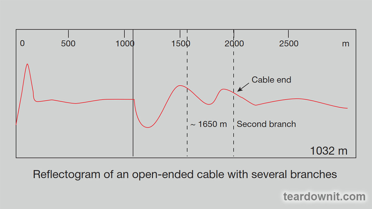 The open end of the cable at a distance of 6500 feet is almost invisible on this reflectogram since the energy of the reflectometer test pulse is spent on passing two branches. If there are multiple branches connected to the cable under test, the best strategy is to locate the first one, access its location, and only then locate the next branch. This procedure should be repeated until the locations of all branches have been found. Let's get to conclusions. Branches obstruct the operation of digital systems. The search for branches and their subsequent removal is extremely important to ensure the high quality of the digital services provided. In order to make sure that the distance to the nearest branch corresponds to the standard for digital lines (maximum and total length of branches), one can use the following algorithm: - Check the distance to the nearest branch. - Check the length of the cable branch. - Check the total length of all branches found. |
| json metadata | {"tags":["aroundcable"],"image":["https://assets-global.website-files.com/6438c93ff266bb9903cab3bc/6614ff5763556ac9df9b98e3_1.jpg","https://assets-global.website-files.com/6438c93ff266bb9903cab3bc/6614ff6024cb1bece4b33682_2.jpg","https://cdn.steemitimages.com/DQmYGDFH1sCpzhqRusf6W9ZS9Y56DmRakExwWseGpYQLm47/image.png","https://cdn.steemitimages.com/DQmZntg3aDEoz45UH5mMUTcBxD26uhe7hHsXUucq5tSxdLC/image.png"],"app":"steemit/0.2","format":"markdown"} |
| parent author | |
| parent permlink | aroundcable |
| permlink | finding-branches-using-a-reflectometer |
| title | Finding branches using a reflectometer |
| Transaction Info | Block #84303694/Trx a5d4794639e7b64f7f51044337d7e2d932e16e48 |
View Raw JSON Data
{
"block": 84303694,
"op": [
"comment",
{
"author": "teardownit",
"body": "As you know, a data cabling system consists of different segments. To connect them all and bring the data connection to the end user, it is necessary to make a certain number of crossings. Often, staff forgets to disconnect \"old\" lines. As a result, over time, parallel branches appear, and their presence can have a detrimental effect on the quality of services.\n\n>BRANCHES AS A SOURCE OF PROBLEMS\n\nParallel branches can make it difficult to serve clients and ensure system functionality. With the introduction of digital systems, the search for parallel branches becomes an increasingly important task since they negatively affect the operation of digital transmission systems and, even if in most cases they are relatively short in length, nevertheless lead to significant problems. The bramch creates a second path for digital signals transmitted on the main line, which travel along the branch and are reflected from its open end. Reflected signals (echoes) enter the main line, where they are mixed with \"good\" digital signals and negatively affect the quality of the transmitted data. Therefore, to ensure correct operation of the digital line, the branches must be disconnected completely.\n\nWhen connecting to analog lines, branching also creates problems. For example, if there is a fault on such a branch, it may show itself in the form of a decrease in the quality of the transmitted signal.\n\nFinally, unknown branches can affect the accuracy of diagnostic equipment, for example, when measuring cable capacitance and estimating the distance to a break using a capacitive bridge. An unknown branch increases the combined capacitance of the cable pair and causes a measurement error: for the tested pair, the calculated length will be greater than the actual length.\n\nIt is very important to have full information about all the parallel branches available on the line in order, if necessary, to select the correct algorithm for troubleshooting and eliminating the problem.\n\nSEARCHING FOR THE LOCATION OF THE BRANCH CONNECTION\nThe capacitive bridge is the device most often used to measure the length of a cable that is open at the far end. Unfortunately, it only allows one to estimate the total length of a cable pair, including all parallel branches.\n\nUsing multi-function devices (combining a capacitive and resistive bridge), it is possible to calculate the length of the branch cable due to the ability to compare the length values obtained from measuring the cable capacitance and the resistance of the loop.\n\nPic main_img_p7621_thumb.png\n\nIn this case, an OTDR is the most optimal and, moreover, the only device that allows one to find the locations of branching, measure the lengths of the branches, and determine the distance to them.\n\nHowever, in practice, cable analyzers that combine the functions of a reflectometer and a multi-function instrument are more convenient. The implementation of two measurement methods (reflectometric and bridge) in one device allows for comparison of the results obtained for more accurate fault localization.\n\nThe classic branch reflectogram is similar to the one for testing a damaged cable, the only difference being that the reflection of the signal from the branch is a straight line rather than a curve.\n\nhttps://assets-global.website-files.com/6438c93ff266bb9903cab3bc/6614ff5763556ac9df9b98e3_1.jpg\n\nAs an explanation, let's look closely at the reflectograms for an open-ended cable section without a branch and a cable section with one (it is located at a distance of 3385 ft). The corresponding measurement results using a capacitive bridge were transferred to the reflectometer for direct comparison and accounted for. Note how the presence of a branch affects the measurement results of a capacitive bridge—in particular, how the cable section with a branch distorts the pulse reflected from the open end of the cable at a distance of 6500 feet. This occurs because part of the energy of the reflectometer signal was lost passing through the branch. The ideal way to view these graphs simultaneously is to use a dual-channel OTDR to connect and compare the \"good\" and \"bad\" cable pairs back-to-back.\n\nhttps://assets-global.website-files.com/6438c93ff266bb9903cab3bc/6614ff6024cb1bece4b33682_2.jpg\n\n\n\nJust as echoes affect digital signal transmission, parallel branches affect cable reflectograms. Interpretation of the reflectogram becomes significantly more difficult if two or more branches are connected to the pair under test.\n\nThe following graph is similar to the one shown in the previous figure, but in this case there is an additional branch at a distance of approximately 5400 feet.\n\n\n\nThe open end of the cable at a distance of 6500 feet is almost invisible on this reflectogram since the energy of the reflectometer test pulse is spent on passing two branches. If there are multiple branches connected to the cable under test, the best strategy is to locate the first one, access its location, and only then locate the next branch. This procedure should be repeated until the locations of all branches have been found.\n\nLet's get to conclusions. Branches obstruct the operation of digital systems. The search for branches and their subsequent removal is extremely important to ensure the high quality of the digital services provided.\n\nIn order to make sure that the distance to the nearest branch corresponds to the standard for digital lines (maximum and total length of branches), one can use the following algorithm:\n\n- Check the distance to the nearest branch.\n- Check the length of the cable branch.\n- Check the total length of all branches found.",
"json_metadata": "{\"tags\":[\"aroundcable\"],\"image\":[\"https://assets-global.website-files.com/6438c93ff266bb9903cab3bc/6614ff5763556ac9df9b98e3_1.jpg\",\"https://assets-global.website-files.com/6438c93ff266bb9903cab3bc/6614ff6024cb1bece4b33682_2.jpg\",\"https://cdn.steemitimages.com/DQmYGDFH1sCpzhqRusf6W9ZS9Y56DmRakExwWseGpYQLm47/image.png\",\"https://cdn.steemitimages.com/DQmZntg3aDEoz45UH5mMUTcBxD26uhe7hHsXUucq5tSxdLC/image.png\"],\"app\":\"steemit/0.2\",\"format\":\"markdown\"}",
"parent_author": "",
"parent_permlink": "aroundcable",
"permlink": "finding-branches-using-a-reflectometer",
"title": "Finding branches using a reflectometer"
}
],
"op_in_trx": 0,
"timestamp": "2024-04-17T07:15:57",
"trx_id": "a5d4794639e7b64f7f51044337d7e2d932e16e48",
"trx_in_block": 4,
"virtual_op": 0
}bluesnipersent 0.010 STEEM to @teardownit- "Hello. Good to see you on Steem. To maximize your rewards, publish your post also on Hive ( hive.blog ) and Blurt ( blurt.blog ) blockchains. Use upvu, jsup or ctime and get instant upvotes"2024/04/10 07:26:36
bluesnipersent 0.010 STEEM to @teardownit- "Hello. Good to see you on Steem. To maximize your rewards, publish your post also on Hive ( hive.blog ) and Blurt ( blurt.blog ) blockchains. Use upvu, jsup or ctime and get instant upvotes"
2024/04/10 07:26:36
| amount | 0.010 STEEM |
| from | bluesniper |
| memo | Hello. Good to see you on Steem. To maximize your rewards, publish your post also on Hive ( hive.blog ) and Blurt ( blurt.blog ) blockchains. Use upvu, jsup or ctime and get instant upvotes |
| to | teardownit |
| Transaction Info | Block #84104672/Trx 9f863082b5551c8ca3c39d2aa2eda16bd20c341a |
View Raw JSON Data
{
  "block": 84104672,
  "op": [
    "transfer",
    {
      "amount": "0.010 STEEM",
      "from": "bluesniper",
      "memo": "Hello. Good to see you on Steem. To maximize your rewards, publish your post also on Hive ( hive.blog ) and Blurt ( blurt.blog ) blockchains. Use upvu, jsup or ctime and get instant upvotes",
      "to": "teardownit"
    }
  ],
  "op_in_trx": 0,
  "timestamp": "2024-04-10T07:26:36",
  "trx_id": "9f863082b5551c8ca3c39d2aa2eda16bd20c341a",
  "trx_in_block": 13,
  "virtual_op": 0
}bluesniperupvoted (100.00%) @teardownit / power-control-unit-for-testing2024/04/10 07:26:15
bluesniperupvoted (100.00%) @teardownit / power-control-unit-for-testing
2024/04/10 07:26:15
| author | teardownit |
| permlink | power-control-unit-for-testing |
| voter | bluesniper |
| weight | 10000 (100.00%) |
| Transaction Info | Block #84104665/Trx bc76af7798bde72c79c5a2675f7969bce8d17537 |
View Raw JSON Data
{
  "block": 84104665,
  "op": [
    "vote",
    {
      "author": "teardownit",
      "permlink": "power-control-unit-for-testing",
      "voter": "bluesniper",
      "weight": 10000
    }
  ],
  "op_in_trx": 0,
  "timestamp": "2024-04-10T07:26:15",
  "trx_id": "bc76af7798bde72c79c5a2675f7969bce8d17537",
  "trx_in_block": 11,
  "virtual_op": 0
}teardownitpublished a new post: power-control-unit-for-testing2024/04/10 07:20:48
teardownitpublished a new post: power-control-unit-for-testing
2024/04/10 07:20:48
| author | teardownit |
| body | >Scheme https://assets-global.website-files.com/6438c93ff266bb9903cab3bc/660d36931bcb76213af7b136_1.jpg Element functions: + J1 - AC grid input + J2 - oscilloscope connection, current monitoring + J3 - output for power supply under test + SW1 - circuit sensitivity switch for measuring Inrush current + SW2 - zero-cross switching on and off + SW3 - instant switching on and off for inrush current measurements + T1 - current transformer, 10A, 1:1000 + U1 - Solid State Relay, zero-cross, controlling voltage 90–250 VAC AC-synchronized switching on and off If the device requires zero-cross on-off switching, the operator should use SW2, while SW3 should be open. In this case, the SW1 should be switched to the lower position according to the diagram. Then, 10A of the grid current will correspond to the connector J2 voltage equal to 1V. In synchronous mode, the on state of SW2 corresponds to a continuous mode; the value of the source current can be easily measured by briefly connecting the ammeter to the output terminals of SSR U1 without changing the position of the switches. With this measurement method, the ammeter does not risk being overloaded by the shock current of turning on the device. Asynchronous switching on and off When measuring INRUSH CURRENT, the operator should reduce the sensitivity of the current measurement circuit (upper position for SW1 on the diagram), open SW2, and use SW3 to turn on the device. In this case, 10A of grid current will correspond to a voltage at connector J2 equal to 0.1V. Since powering on will be accidental relative to the source phase, the measurement procedure should be repeated several times (at least ten). Only then can the maximum and average values for the INRUSH CURRENT be reliably determined. >Assembly The described power control unit was assembled on a breadboard with a 0.1-inch pitch; the look of the unit is shown in the photos below: On view 1 of the power control unit in the foreground, one can find the terminals for connecting the source and the device under test, switch SW2, and current transformer T1:  Power control unit view 2:  Power control unit view 3 shows the current sensitivity switch SW1 and connector J2:  Usage example For example, if one uses the device to test a power supply, then with an oscilloscope, one can determine the following characteristics of the unit: INRUSH CURRENT Peak input current at full load POWER FACTOR Power factor of AC mains draw (usually listed if there is a PFC in the supply) https://en.wikipedia.org/wiki/Power_factor SETUP TIME Time to set up from the moment of applying the input voltage until the output voltage reaches 90% of the rated level at 100% load. RISE TIME Time for the output voltage to rise from 10% to 90% of the nominal level. HOLD UP TIME Time to keep operating at 100% load from the moment the input voltage is turned off until the output voltage drops to 90% of the rated level. FALL TIME The output voltage decay time is 90% to 10% of the nominal level. ======== Done. Best regards. |
| json metadata | {"tags":["powertesting"],"image":["https://assets-global.website-files.com/6438c93ff266bb9903cab3bc/660d36931bcb76213af7b136_1.jpg","https://cdn.steemitimages.com/DQmbaCoqoLN4jn4aeBJEELrq1Kmw4zNmtC2gJp3YAAqUC7j/image.png","https://cdn.steemitimages.com/DQmet2KsKPgVwqthhEZockSs3R6ZNELG6j9QNDdJMr7gSpX/image.png","https://cdn.steemitimages.com/DQmeeiW3nrfBvhgCCRUtvwgad1df1ULA7Ls6NhEjKkv3Vfs/image.png"],"links":["https://en.wikipedia.org/wiki/Power_factor"],"app":"steemit/0.2","format":"markdown"} |
| parent author | |
| parent permlink | powertesting |
| permlink | power-control-unit-for-testing |
| title | Power control unit for testing |
| Transaction Info | Block #84104561/Trx 9e6a54a2f2ce029f98bbbacc1ed38184b67d709e |
View Raw JSON Data
{
"block": 84104561,
"op": [
"comment",
{
"author": "teardownit",
"body": ">Scheme\nhttps://assets-global.website-files.com/6438c93ff266bb9903cab3bc/660d36931bcb76213af7b136_1.jpg\n\nElement functions:\n\n+ J1 - AC grid input \n+ J2 - oscilloscope connection, current monitoring\n+ J3 - output for power supply under test\n+ SW1 - circuit sensitivity switch for measuring Inrush current\n+ SW2 - zero-cross switching on and off\n+ SW3 - instant switching on and off for inrush current measurements\n+ T1 - current transformer, 10A, 1:1000\n+ U1 - Solid State Relay, zero-cross, controlling voltage 90–250 VAC\n\nAC-synchronized switching on and off\n\nIf the device requires zero-cross on-off switching, the operator should use SW2, while SW3 should be open. In this case, the SW1 should be switched to the lower position according to the diagram. Then, 10A of the grid current will correspond to the connector J2 voltage equal to 1V.\n\nIn synchronous mode, the on state of SW2 corresponds to a continuous mode; the value of the source current can be easily measured by briefly connecting the ammeter to the output terminals of SSR U1 without changing the position of the switches. With this measurement method, the ammeter does not risk being overloaded by the shock current of turning on the device.\n\nAsynchronous switching on and off\nWhen measuring INRUSH CURRENT, the operator should reduce the sensitivity of the current measurement circuit (upper position for SW1 on the diagram), open SW2, and use SW3 to turn on the device. In this case, 10A of grid current will correspond to a voltage at connector J2 equal to 0.1V.\n\nSince powering on will be accidental relative to the source phase, the measurement procedure should be repeated several times (at least ten). Only then can the maximum and average values for the INRUSH CURRENT be reliably determined.\n\n>Assembly\n\nThe described power control unit was assembled on a breadboard with a 0.1-inch pitch; the look of the unit is shown in the photos below:\n\nOn view 1 of the power control unit in the foreground, one can find the terminals for connecting the source and the device under test, switch SW2, and current transformer T1:\n\n\n\n\nPower control unit view 2:\n\n\n\n\n\nPower control unit view 3 shows the current sensitivity switch SW1 and connector J2:\n\n\n\n\nUsage example\nFor example, if one uses the device to test a power supply, then with an oscilloscope, one can determine the following characteristics of the unit:\n\nINRUSH CURRENT\nPeak input current at full load\n\nPOWER FACTOR\nPower factor of AC mains draw (usually listed if there is a PFC in the supply) https://en.wikipedia.org/wiki/Power_factor\n\nSETUP TIME\nTime to set up from the moment of applying the input voltage until the output voltage reaches 90% of the rated level at 100% load.\n\nRISE TIME\nTime for the output voltage to rise from 10% to 90% of the nominal level.\n\nHOLD UP TIME\nTime to keep operating at 100% load from the moment the input voltage is turned off until the output voltage drops to 90% of the rated level.\n\nFALL TIME\nThe output voltage decay time is 90% to 10% of the nominal level.\n\n========\n\nDone.\nBest regards.",
"json_metadata": "{\"tags\":[\"powertesting\"],\"image\":[\"https://assets-global.website-files.com/6438c93ff266bb9903cab3bc/660d36931bcb76213af7b136_1.jpg\",\"https://cdn.steemitimages.com/DQmbaCoqoLN4jn4aeBJEELrq1Kmw4zNmtC2gJp3YAAqUC7j/image.png\",\"https://cdn.steemitimages.com/DQmet2KsKPgVwqthhEZockSs3R6ZNELG6j9QNDdJMr7gSpX/image.png\",\"https://cdn.steemitimages.com/DQmeeiW3nrfBvhgCCRUtvwgad1df1ULA7Ls6NhEjKkv3Vfs/image.png\"],\"links\":[\"https://en.wikipedia.org/wiki/Power_factor\"],\"app\":\"steemit/0.2\",\"format\":\"markdown\"}",
"parent_author": "",
"parent_permlink": "powertesting",
"permlink": "power-control-unit-for-testing",
"title": "Power control unit for testing"
}
],
"op_in_trx": 0,
"timestamp": "2024-04-10T07:20:48",
"trx_id": "9e6a54a2f2ce029f98bbbacc1ed38184b67d709e",
"trx_in_block": 2,
"virtual_op": 0
}bluesnipersent 0.010 STEEM to @teardownit- "Hello. Good to see you on Steem. To maximize your rewards, publish your post also on Hive ( hive.blog ) and Blurt ( blurt.blog ) blockchains. Use upvu, jsup or ctime and get instant upvotes"2024/04/03 07:57:39
bluesnipersent 0.010 STEEM to @teardownit- "Hello. Good to see you on Steem. To maximize your rewards, publish your post also on Hive ( hive.blog ) and Blurt ( blurt.blog ) blockchains. Use upvu, jsup or ctime and get instant upvotes"
2024/04/03 07:57:39
| amount | 0.010 STEEM |
| from | bluesniper |
| memo | Hello. Good to see you on Steem. To maximize your rewards, publish your post also on Hive ( hive.blog ) and Blurt ( blurt.blog ) blockchains. Use upvu, jsup or ctime and get instant upvotes |
| to | teardownit |
| Transaction Info | Block #83905165/Trx 889eb2d065b452a9c0a7cd07c215b0ebdb1833d6 |
View Raw JSON Data
{
  "block": 83905165,
  "op": [
    "transfer",
    {
      "amount": "0.010 STEEM",
      "from": "bluesniper",
      "memo": "Hello. Good to see you on Steem. To maximize your rewards, publish your post also on Hive ( hive.blog ) and Blurt ( blurt.blog ) blockchains. Use upvu, jsup or ctime and get instant upvotes",
      "to": "teardownit"
    }
  ],
  "op_in_trx": 0,
  "timestamp": "2024-04-03T07:57:39",
  "trx_id": "889eb2d065b452a9c0a7cd07c215b0ebdb1833d6",
  "trx_in_block": 13,
  "virtual_op": 0
}bluesniperupvoted (100.00%) @teardownit / marshall-guv-nor-a-pedal-that-sounds-like-a-tube-stack2024/04/03 07:57:18
bluesniperupvoted (100.00%) @teardownit / marshall-guv-nor-a-pedal-that-sounds-like-a-tube-stack
2024/04/03 07:57:18
| author | teardownit |
| permlink | marshall-guv-nor-a-pedal-that-sounds-like-a-tube-stack |
| voter | bluesniper |
| weight | 10000 (100.00%) |
| Transaction Info | Block #83905158/Trx 72c11cc0a5af748fba9873afa94458009ebc210e |
View Raw JSON Data
{
  "block": 83905158,
  "op": [
    "vote",
    {
      "author": "teardownit",
      "permlink": "marshall-guv-nor-a-pedal-that-sounds-like-a-tube-stack",
      "voter": "bluesniper",
      "weight": 10000
    }
  ],
  "op_in_trx": 0,
  "timestamp": "2024-04-03T07:57:18",
  "trx_id": "72c11cc0a5af748fba9873afa94458009ebc210e",
  "trx_in_block": 4,
  "virtual_op": 0
}teardownitpublished a new post: marshall-guv-nor-a-pedal-that-sounds-like-a-tube-stack2024/04/03 07:51:39
teardownitpublished a new post: marshall-guv-nor-a-pedal-that-sounds-like-a-tube-stack
2024/04/03 07:51:39
| author | teardownit |
| body |  To be more accurate, it sounds like a valve stack; after all, it is a British pedal imitating British Marshall amplifiers. https://assets-global.website-files.com/6438c93ff266bb9903cab3bc/660173a2d96eb798678c7e8d_1.jpg Don't tell anyone because it's a secret: when creating his JTM45, Jim Marshall actually copied the circuitry of a 1959 Fender Tweed Bassman 5F6-A.  And Mr. Marshall also equipped his first 50-watt combo amplifier, a 1961 JMP Tremolo “Bluesbreaker,” with four 10-inch speakers. The iconic 2x12" version was made a year later.  Tolex instead of tweed, a horizontal arrangement of tubes, and ring-shaped loudspeaker magnets—the differences end there. But why does the British Marshall sound so different from the American Fender? Is the difference really just the Celestion speakers instead of the Jenhsen ones with their U-shaped magnetic core? https://assets-global.website-files.com/6438c93ff266bb9903cab3bc/660173b8b42ffaa2cef14f03_4.jpg The stronger magnetic field of British loudspeakers compresses the sound's dynamic range to a significant extent. One can compare the waveforms recorded with the Shure SM57 microphone from the 12" Celestion G12M Greenback and Fender Mustang II (V1) loudspeakers, as well as from the 8" Orange Voice of the World PPC108. But the spiciest part of the Marshall sound is literally based on the usage of British valves instead of American tubes. https://assets-global.website-files.com/6438c93ff266bb9903cab3bc/660174ebbf41174cc5727db9_6.jpg In the post about a simple DIY tube guitar amplifier, we already noted that the sound of a particular tube depends on the geometry of the grids and anode. https://assets-global.website-files.com/6438c93ff266bb9903cab3bc/660173bea28c652280edb266_5.jpg And if we compare 12AX7 preamp tubes with ECC83, we will see and hear that they are all very different. This is determined not by an American or European stamp but by the design of this particular unit from a particular manufacturer. https://assets-global.website-files.com/6438c93ff266bb9903cab3bc/6601740bb42ffaa2cef19a79_7.jpg It's a completely different story with the EL34 and 6L6 power amplification output tubes. Their sound difference is on another level. Short and thick American 6L6 can be described as high fidelity with a large headroom; long and thin English EL34 is, on the contrary, a growling and roaring powerhouse due to the fact that it tends to limit and distort the signal. Does this mean that if you swap the speakers and tubes in the Tweed Bassman and Bluesbreaker combos, the Fender 5F6-A would become a Marshall JTM45? Not really, no. In the universe of guitar amplification, nuances matter: the cabinet's open or closed back wall, the fine selection of component values, and the frequencies to which the tone controls are set. And, of course, the sound is influenced by the anode supply rectifiers and the supply and output transformers. And according to some experts, even the material of the chassis matters: the windings of transformers have considerable leakage inductance, and their alternating magnetic field interacts with the metal of the chassis. Then there's another question: is it possible to emulate all these effects without real tubes, bulky loudspeakers, and heavy multi-pound transformers? A guitar amplifier is a complex yet still measurable device; it's subject to the laws of physics and can be mathematically evaluated. There is no doubt about the possibility of recreating a certain sound by other means. The question is how complex the circuit with transistors and ICs will be sufficient to obtain a convincing effect. The idea to replicate the iconic sound of the Marshall JTM 45 and JCM800 in a pedal body and create the world's first amp-in-a-box, oddly enough, first came to none other than the employees of the Marshall company itself, led by the head of the Development Department, Steve Grindrod. Guitarists worldwide owe a debt of gratitude to this man for developing the legendary Marshall JCM800 and Vox AC30. https://assets-global.website-files.com/6438c93ff266bb9903cab3bc/6601742c655f481b5330dfe3_9.jpg Today, the godfather of British Sound owns his company, Steve Grindrod (Albion) Amplification. He produces Pendragon guitar amps and Gypsy Boy acoustic amps and works with various charities. And in 1988, his efforts led to the creation of the Guv’nor pedal. https://assets-global.website-files.com/6438c93ff266bb9903cab3bc/66017436960f138d1b13651a_10.jpg In 1992, the pedal was re-released under the name Drive Master. It differed from the original only without an effects loop jack. The circuit looks like a regular distortion pedal with two operational amplifiers. The first is included as a non-inverting amplifier; the signal is supplied to the non-inverting input. And the second operational amplifier is used in the inverting connection. https://assets-global.website-files.com/6438c93ff266bb9903cab3bc/6601743d4dd5cb4a7b397396_11.jpg The drive regulator potentiometer is configured to control the negative feedback of both op-amps. This is a brilliant design by Steve Grindrod. https://assets-global.website-files.com/6438c93ff266bb9903cab3bc/660174445ed3ed861a4fe6c8_12.jpg By comparison, Orange tube and transistor amplifiers typically use dual, linked potentiometers to control the gain of the two stages simultaneously.  Red LEDs are used as limiting elements in this Marshall amp-in-a-box. This makes it possible to adjust overdrive and compression using the drive knob in a wider range and get a sound from light blues overdrive to hard heavy metal distortion. And, of course, the standout feature of this pedal is the gorgeous three-way tone stack, tuned for that signature Marshall sound. It has even more components than the tone stacks of many other tube amps. This happens because the pedal does not have as many gain stages, each with timbre-shaping frequency-dependent circuits, as a large amplifier does. The tone stack has more work to do in the pedal than in the amp head or combo. At least, that's what Steve Grindrod thought when developing The Guv'nor. However, in 1992, when developing the Blues Breaker pedal, it turned out that the distortion sounded great with just one tone knob, a simple treble-bleed circuit. Three new pedals were developed. Drive Master was a reissue of The Guv'nor. Blues Breaker featured soft clipping and lower gain. https://assets-global.website-files.com/6438c93ff266bb9903cab3bc/66017454e746248f784f67e2_14.jpg The Shred Master, on the other hand, was a pedal with maximum gain and a Contour knob, which allowed to emphasize the mids for a vintage sound or, alternatively, make a mid scoop and get a modern sound. As any successful pedal deserves, The Guv’nor was soon copied by other manufacturers: Daddy O from Danelectro, Crunch Box from MI Audio, Riot from Suhr, and Angry Charlie from JHS. Different versions of these pedals may have a three-way tone stack or a single-tone knob, a switch or presence control in the form of a knob or trim pot inside the body, and a limiting diode switch that sets the compression depth.  The version I put together has four knobs: gain, volume, tone, and presence. I enjoy how this pedal sounds with different guitars. In the video, I play a 2011 Gibson MM Explorer. https://youtu.be/7btB4CLhBfY Suppose you want to add Marshall-style voicing to your rig and get some bright British crunch. In that case, you should consider purchasing or building one of the pedals based on the Marshall Guv`nor circuit. |
| json metadata | {"tags":["diy"],"image":["https://cdn.steemitimages.com/DQmPWc6tRNG4aEoHaKcMTDFdTpHx5vsokTcenHpbLtJNVbb/image.png","https://assets-global.website-files.com/6438c93ff266bb9903cab3bc/660173a2d96eb798678c7e8d_1.jpg","https://cdn.steemitimages.com/DQmYB12aYqtLmwf9ewQWZW9cyAmtKUMXErmWV4gALKHrF5z/image.png","https://cdn.steemitimages.com/DQmdGdA85kpb3Ru5wxzo6TLSkntp5pK6FoEQ1uo7HVNUDdL/image.png","https://assets-global.website-files.com/6438c93ff266bb9903cab3bc/660173b8b42ffaa2cef14f03_4.jpg","https://assets-global.website-files.com/6438c93ff266bb9903cab3bc/660174ebbf41174cc5727db9_6.jpg","https://assets-global.website-files.com/6438c93ff266bb9903cab3bc/660173bea28c652280edb266_5.jpg","https://assets-global.website-files.com/6438c93ff266bb9903cab3bc/6601740bb42ffaa2cef19a79_7.jpg","https://assets-global.website-files.com/6438c93ff266bb9903cab3bc/6601742c655f481b5330dfe3_9.jpg","https://assets-global.website-files.com/6438c93ff266bb9903cab3bc/66017436960f138d1b13651a_10.jpg","https://assets-global.website-files.com/6438c93ff266bb9903cab3bc/6601743d4dd5cb4a7b397396_11.jpg","https://assets-global.website-files.com/6438c93ff266bb9903cab3bc/660174445ed3ed861a4fe6c8_12.jpg","https://cdn.steemitimages.com/DQmcVsf4vreinmYoh6Njuty19ewAQ3Wk6HZ38Z1AHYZyojh/image.png","https://assets-global.website-files.com/6438c93ff266bb9903cab3bc/66017454e746248f784f67e2_14.jpg","https://cdn.steemitimages.com/DQmcDddgvYAj4yYgpv7KYsjs6c5FL134rNGYuEJxbYDofBJ/image.png","https://img.youtube.com/vi/7btB4CLhBfY/0.jpg"],"links":["https://youtu.be/7btB4CLhBfY"],"app":"steemit/0.2","format":"markdown"} |
| parent author | |
| parent permlink | diy |
| permlink | marshall-guv-nor-a-pedal-that-sounds-like-a-tube-stack |
| title | Marshall Guv`nor: a Pedal that sounds like a Tube Stack |
| Transaction Info | Block #83905045/Trx 0fc139e8674520ead1d883db76e297475c58f9ff |
View Raw JSON Data
{
"block": 83905045,
"op": [
"comment",
{
"author": "teardownit",
"body": "\n\nTo be more accurate, it sounds like a valve stack; after all, it is a British pedal imitating British Marshall amplifiers.\n\nhttps://assets-global.website-files.com/6438c93ff266bb9903cab3bc/660173a2d96eb798678c7e8d_1.jpg\n\nDon't tell anyone because it's a secret: when creating his JTM45, Jim Marshall actually copied the circuitry of a 1959 Fender Tweed Bassman 5F6-A.\n\n\n\nAnd Mr. Marshall also equipped his first 50-watt combo amplifier, a 1961 JMP Tremolo “Bluesbreaker,” with four 10-inch speakers. The iconic 2x12\" version was made a year later.\n\n\n\nTolex instead of tweed, a horizontal arrangement of tubes, and ring-shaped loudspeaker magnets—the differences end there.\n\nBut why does the British Marshall sound so different from the American Fender? Is the difference really just the Celestion speakers instead of the Jenhsen ones with their U-shaped magnetic core?\n\nhttps://assets-global.website-files.com/6438c93ff266bb9903cab3bc/660173b8b42ffaa2cef14f03_4.jpg\n\nThe stronger magnetic field of British loudspeakers compresses the sound's dynamic range to a significant extent. One can compare the waveforms recorded with the Shure SM57 microphone from the 12\" Celestion G12M Greenback and Fender Mustang II (V1) loudspeakers, as well as from the 8\" Orange Voice of the World PPC108.\n\nBut the spiciest part of the Marshall sound is literally based on the usage of British valves instead of American tubes.\n\nhttps://assets-global.website-files.com/6438c93ff266bb9903cab3bc/660174ebbf41174cc5727db9_6.jpg\n\nIn the post about a simple DIY tube guitar amplifier, we already noted that the sound of a particular tube depends on the geometry of the grids and anode.\n\nhttps://assets-global.website-files.com/6438c93ff266bb9903cab3bc/660173bea28c652280edb266_5.jpg\n\nAnd if we compare 12AX7 preamp tubes with ECC83, we will see and hear that they are all very different. This is determined not by an American or European stamp but by the design of this particular unit from a particular manufacturer.\n\nhttps://assets-global.website-files.com/6438c93ff266bb9903cab3bc/6601740bb42ffaa2cef19a79_7.jpg\n\nIt's a completely different story with the EL34 and 6L6 power amplification output tubes. Their sound difference is on another level. Short and thick American 6L6 can be described as high fidelity with a large headroom; long and thin English EL34 is, on the contrary, a growling and roaring powerhouse due to the fact that it tends to limit and distort the signal.\n\nDoes this mean that if you swap the speakers and tubes in the Tweed Bassman and Bluesbreaker combos, the Fender 5F6-A would become a Marshall JTM45? Not really, no.\n\nIn the universe of guitar amplification, nuances matter: the cabinet's open or closed back wall, the fine selection of component values, and the frequencies to which the tone controls are set.\n\nAnd, of course, the sound is influenced by the anode supply rectifiers and the supply and output transformers. And according to some experts, even the material of the chassis matters: the windings of transformers have considerable leakage inductance, and their alternating magnetic field interacts with the metal of the chassis.\n\nThen there's another question: is it possible to emulate all these effects without real tubes, bulky loudspeakers, and heavy multi-pound transformers? A guitar amplifier is a complex yet still measurable device; it's subject to the laws of physics and can be mathematically evaluated.\n\nThere is no doubt about the possibility of recreating a certain sound by other means. The question is how complex the circuit with transistors and ICs will be sufficient to obtain a convincing effect.\n\nThe idea to replicate the iconic sound of the Marshall JTM 45 and JCM800 in a pedal body and create the world's first amp-in-a-box, oddly enough, first came to none other than the employees of the Marshall company itself, led by the head of the Development Department, Steve Grindrod.\n\nGuitarists worldwide owe a debt of gratitude to this man for developing the legendary Marshall JCM800 and Vox AC30.\n\nhttps://assets-global.website-files.com/6438c93ff266bb9903cab3bc/6601742c655f481b5330dfe3_9.jpg\n\nToday, the godfather of British Sound owns his company, Steve Grindrod (Albion) Amplification. He produces Pendragon guitar amps and Gypsy Boy acoustic amps and works with various charities. And in 1988, his efforts led to the creation of the Guv’nor pedal.\n\nhttps://assets-global.website-files.com/6438c93ff266bb9903cab3bc/66017436960f138d1b13651a_10.jpg\n\nIn 1992, the pedal was re-released under the name Drive Master. It differed from the original only without an effects loop jack.\n\nThe circuit looks like a regular distortion pedal with two operational amplifiers. The first is included as a non-inverting amplifier; the signal is supplied to the non-inverting input. And the second operational amplifier is used in the inverting connection.\n\nhttps://assets-global.website-files.com/6438c93ff266bb9903cab3bc/6601743d4dd5cb4a7b397396_11.jpg\n\nThe drive regulator potentiometer is configured to control the negative feedback of both op-amps. This is a brilliant design by Steve Grindrod.\n\nhttps://assets-global.website-files.com/6438c93ff266bb9903cab3bc/660174445ed3ed861a4fe6c8_12.jpg\n\nBy comparison, Orange tube and transistor amplifiers typically use dual, linked potentiometers to control the gain of the two stages simultaneously.\n\n\nRed LEDs are used as limiting elements in this Marshall amp-in-a-box. This makes it possible to adjust overdrive and compression using the drive knob in a wider range and get a sound from light blues overdrive to hard heavy metal distortion.\n\nAnd, of course, the standout feature of this pedal is the gorgeous three-way tone stack, tuned for that signature Marshall sound. It has even more components than the tone stacks of many other tube amps.\n\nThis happens because the pedal does not have as many gain stages, each with timbre-shaping frequency-dependent circuits, as a large amplifier does. The tone stack has more work to do in the pedal than in the amp head or combo. At least, that's what Steve Grindrod thought when developing The Guv'nor.\n\nHowever, in 1992, when developing the Blues Breaker pedal, it turned out that the distortion sounded great with just one tone knob, a simple treble-bleed circuit.\n\nThree new pedals were developed. Drive Master was a reissue of The Guv'nor. Blues Breaker featured soft clipping and lower gain.\n\nhttps://assets-global.website-files.com/6438c93ff266bb9903cab3bc/66017454e746248f784f67e2_14.jpg\n\nThe Shred Master, on the other hand, was a pedal with maximum gain and a Contour knob, which allowed to emphasize the mids for a vintage sound or, alternatively, make a mid scoop and get a modern sound.\n\nAs any successful pedal deserves, The Guv’nor was soon copied by other manufacturers: Daddy O from Danelectro, Crunch Box from MI Audio, Riot from Suhr, and Angry Charlie from JHS.\n\nDifferent versions of these pedals may have a three-way tone stack or a single-tone knob, a switch or presence control in the form of a knob or trim pot inside the body, and a limiting diode switch that sets the compression depth.\n\n\n\nThe version I put together has four knobs: gain, volume, tone, and presence. I enjoy how this pedal sounds with different guitars. In the video, I play a 2011 Gibson MM Explorer.\n\nhttps://youtu.be/7btB4CLhBfY\n\nSuppose you want to add Marshall-style voicing to your rig and get some bright British crunch. In that case, you should consider purchasing or building one of the pedals based on the Marshall Guv`nor circuit.",
"json_metadata": "{\"tags\":[\"diy\"],\"image\":[\"https://cdn.steemitimages.com/DQmPWc6tRNG4aEoHaKcMTDFdTpHx5vsokTcenHpbLtJNVbb/image.png\",\"https://assets-global.website-files.com/6438c93ff266bb9903cab3bc/660173a2d96eb798678c7e8d_1.jpg\",\"https://cdn.steemitimages.com/DQmYB12aYqtLmwf9ewQWZW9cyAmtKUMXErmWV4gALKHrF5z/image.png\",\"https://cdn.steemitimages.com/DQmdGdA85kpb3Ru5wxzo6TLSkntp5pK6FoEQ1uo7HVNUDdL/image.png\",\"https://assets-global.website-files.com/6438c93ff266bb9903cab3bc/660173b8b42ffaa2cef14f03_4.jpg\",\"https://assets-global.website-files.com/6438c93ff266bb9903cab3bc/660174ebbf41174cc5727db9_6.jpg\",\"https://assets-global.website-files.com/6438c93ff266bb9903cab3bc/660173bea28c652280edb266_5.jpg\",\"https://assets-global.website-files.com/6438c93ff266bb9903cab3bc/6601740bb42ffaa2cef19a79_7.jpg\",\"https://assets-global.website-files.com/6438c93ff266bb9903cab3bc/6601742c655f481b5330dfe3_9.jpg\",\"https://assets-global.website-files.com/6438c93ff266bb9903cab3bc/66017436960f138d1b13651a_10.jpg\",\"https://assets-global.website-files.com/6438c93ff266bb9903cab3bc/6601743d4dd5cb4a7b397396_11.jpg\",\"https://assets-global.website-files.com/6438c93ff266bb9903cab3bc/660174445ed3ed861a4fe6c8_12.jpg\",\"https://cdn.steemitimages.com/DQmcVsf4vreinmYoh6Njuty19ewAQ3Wk6HZ38Z1AHYZyojh/image.png\",\"https://assets-global.website-files.com/6438c93ff266bb9903cab3bc/66017454e746248f784f67e2_14.jpg\",\"https://cdn.steemitimages.com/DQmcDddgvYAj4yYgpv7KYsjs6c5FL134rNGYuEJxbYDofBJ/image.png\",\"https://img.youtube.com/vi/7btB4CLhBfY/0.jpg\"],\"links\":[\"https://youtu.be/7btB4CLhBfY\"],\"app\":\"steemit/0.2\",\"format\":\"markdown\"}",
"parent_author": "",
"parent_permlink": "diy",
"permlink": "marshall-guv-nor-a-pedal-that-sounds-like-a-tube-stack",
"title": "Marshall Guv`nor: a Pedal that sounds like a Tube Stack"
}
],
"op_in_trx": 0,
"timestamp": "2024-04-03T07:51:39",
"trx_id": "0fc139e8674520ead1d883db76e297475c58f9ff",
"trx_in_block": 1,
"virtual_op": 0
}teardownitpublished a new post: hdmi-standard-and-functions2024/03/29 08:22:21
teardownitpublished a new post: hdmi-standard-and-functions
2024/03/29 08:22:21
| author | teardownit |
| body | HDMI stands for high-definition multimedia interface. Since it has HD in the name, it should be easy for anyone to guess when it was first introduced and implemented, raising 'HD' on the flag is so early 2000s. HDMI is a digital interface that was and still is competing with DisplayPort. The crucial thing in this standoff was that DisplayPort was always meant for computers and all the alike. At the same time, HDMI was developed by a consortium of consumer tech manufacturers, including TV makers. Historically, this meant a much greater spread of the technology, so any new type of device should have HDMI if it supports an external display for any purpose. https://assets-global.website-files.com/6438c93ff266bb9903cab3bc/65fc2e431df9fe2e5d1b8db3_image-11.jpg HD am I, image source: Reddit, r/puns Just to keep this explanation fair, DisplayPort still has one undoubtedly significant advantage—native support for Thunderbolt USB-C. Thunderbolt and USB-C are complex standards, so I won't dive deep into this. It should be noted that if you have a fairly recently produced laptop computer with USB-C, then connecting it with a USB-C to DisplayPort cable is simpler compared to a USB-C to HDMI converter. This makes no difference to 99% of users, but an unnecessary converter can bother some. All that aside, back to the topic. HDMI has gone through several versions. Usable (or, should I say, meaningful) ones right now are 1.4b, 2.0, and 2.1. This hot take and all the following could be technically incorrect, but are a good rule of thumb to evaluate cables and devices: HDMI 1.4b is a version with a 10 Gb/s transmission rate, used for FullHD (and up to 1440p with some limitations) and basic additional functions like HDCP, ARC, Ethernet, and CEC. HDCP is a content protection protocol used from the beginning of HDMI and is closely tied to it. In simple terms, it is here to ensure that the system's endpoint is indeed a monitor and not streaming or recording equipment. Suppose one tries to stream an HDCP-protected Netflix show from a laptop to a streaming box with no HDCP support (like some enterprise screen-sharing solutions). In that case, the image on the screen will be just black. ARC stands for 'audio return channel'; video and audio signals are sent to the TV, video is shown, and audio is transmitted back through the same HDMI cable to be played on the player's, console, or PC side. The easy way to play sound on some standalone audio system instead of TV speakers is, of course, a trusted audio jack output on the TV. Using ARC is the right way to do it with an amp or an audio receiver near the media player. HDMI audio could be multi-channel, but the one-eight-inch stereo port is limited to just two channels. Ethernet is an excellent addition to video and was added to the standard relatively early. It can be implemented on a single twisted pair inside an HDMI cable. Ethernet over HDMI is neither fast nor widespread, so the idea of ditching ARC and CEC (those wires are used for Ethernet) did not take off. CEC is a basic, unified list of commands for consumer electronics, like 'on', 'off', 'switch to input 1', etc. CEC control is a type of protocol that requires no input from the user, and due to its simplicity, it is quietly implemented in most consumer media players. When the streaming starts, any Chromecast-like device does not hesitate to send out a few bytes to the TV to wake it from standby and switch to the appropriate input. HDMI 2.0 is the one with 18 Gb/s throughput. This version can deliver 4K 30 frames per second with no color compression or up to 4K 60 fps with slightly reduced color space and no HDR. So if you plan on using a budget-friendly TV or a monitor—not a crazy bright one, not connected to a top-of-the-line gaming rig capable of outputting 4K at 120+ fps—then HDMI 2.0 transmitters, cables, and switches are fine. But if you do, then the next version is for you. Additional functions are static HDR (for 2.0a, dynamic for 2.0b), better and more capable CEC, and ARC. 'No color compression' means using the full 4:4:4 YCbCr color space. Number sequences 4:2:0 and 4:2:2 represent different levels of compression: the same level of luminance and less accurate colors are made so that the average consumer does not see the difference. Certain edge cases can become apparent, especially when displaying color gradients. 4:2:2 is primarily fine for watching any content or playing games; working with text and numbers needs 4:4:4 as all the fonts are fine-tuned to be displayed with no compression and require every pixel to be exactly right in terms of color and intensity to look good. HDR stands for 'high dynamic range' and is a widely marketed feature. HDR means more light in general and more luminance levels for cinematic night shots, sunsets, and fire. HDMI 2.1—more than 40 Gb/s of data for 4K and 5K resolutions with high frame rates and no limitations, or up to the still rarely used 8K. As the resolution is still 4K, as in the previous version, added HDMI functions are centered around supporting variable frame rate (VRR) and improving color accuracy and sound quality. HDMI 2.1 takes up to 40-48 Gb/s. It has all the bells and whistles imaginable; the latest version came out in August 2023. In terms of comparison, HDMI 2.1 supports 4K and 5K (up to 10K, but it's expensive to test) with high frame rates, HDR, and many audio channels transmitted forward and backward. So, for now, it should be considered future-proofing the video system to be used long after purchase to its fullest. https://assets-global.website-files.com/6438c93ff266bb9903cab3bc/65fc2e5f59858f314ab7b4fd_image-12.jpg 4K60, HDMI 2.0, non-HDR wireless extender, Inrix In conclusion, the TLDR is this: HDMI is standardized in terms of resolution and frames per second, but many functions are just optional. Switchers, TVs, and cables should support HDMI 1.4, 2.0, or 2.1 (this corresponds to resolution and fps support) and list all the supported functions. Keep in mind that 'ARC' can be googled and is a valid function; 'low-noise' and 'exceptional image quality' are not. ====== Eugenio S |
| json metadata | {"tags":["hdmi"],"image":["https://assets-global.website-files.com/6438c93ff266bb9903cab3bc/65fc2e431df9fe2e5d1b8db3_image-11.jpg","https://assets-global.website-files.com/6438c93ff266bb9903cab3bc/65fc2e5f59858f314ab7b4fd_image-12.jpg"],"app":"steemit/0.2","format":"markdown"} |
| parent author | |
| parent permlink | hdmi |
| permlink | hdmi-standard-and-functions |
| title | HDMI standard and functions |
| Transaction Info | Block #83763010/Trx c488b90022f292e33f846f26435d5cc914e51b75 |
View Raw JSON Data
{
  "block": 83763010,
  "op": [
    "comment",
    {
      "author": "teardownit",
      "body": "HDMI stands for high-definition multimedia interface. Since it has HD in the name, it should be easy for anyone to guess when it was first introduced and implemented, raising 'HD' on the flag is so early 2000s. HDMI is a digital interface that was and still is competing with DisplayPort. The crucial thing in this standoff was that DisplayPort was always meant for computers and all the alike. At the same time, HDMI was developed by a consortium of consumer tech manufacturers, including TV makers. Historically, this meant a much greater spread of the technology, so any new type of device should have HDMI if it supports an external display for any purpose.\n\nhttps://assets-global.website-files.com/6438c93ff266bb9903cab3bc/65fc2e431df9fe2e5d1b8db3_image-11.jpg\nHD am I, image source: Reddit, r/puns\n\nJust to keep this explanation fair, DisplayPort still has one undoubtedly significant advantage—native support for Thunderbolt USB-C. Thunderbolt and USB-C are complex standards, so I won't dive deep into this. It should be noted that if you have a fairly recently produced laptop computer with USB-C, then connecting it with a USB-C to DisplayPort cable is simpler compared to a USB-C to HDMI converter. This makes no difference to 99% of users, but an unnecessary converter can bother some.\n\nAll that aside, back to the topic. HDMI has gone through several versions. Usable (or, should I say, meaningful) ones right now are 1.4b, 2.0, and 2.1. This hot take and all the following could be technically incorrect, but are a good rule of thumb to evaluate cables and devices:\n\nHDMI 1.4b is a version with a 10 Gb/s transmission rate, used for FullHD (and up to 1440p with some limitations) and basic additional functions like HDCP, ARC, Ethernet, and CEC.\n\nHDCP is a content protection protocol used from the beginning of HDMI and is closely tied to it. In simple terms, it is here to ensure that the system's endpoint is indeed a monitor and not streaming or recording equipment. Suppose one tries to stream an HDCP-protected Netflix show from a laptop to a streaming box with no HDCP support (like some enterprise screen-sharing solutions). In that case, the image on the screen will be just black.\n\nARC stands for 'audio return channel'; video and audio signals are sent to the TV, video is shown, and audio is transmitted back through the same HDMI cable to be played on the player's, console, or PC side. The easy way to play sound on some standalone audio system instead of TV speakers is, of course, a trusted audio jack output on the TV. Using ARC is the right way to do it with an amp or an audio receiver near the media player. HDMI audio could be multi-channel, but the one-eight-inch stereo port is limited to just two channels.\n\nEthernet is an excellent addition to video and was added to the standard relatively early. It can be implemented on a single twisted pair inside an HDMI cable. Ethernet over HDMI is neither fast nor widespread, so the idea of ditching ARC and CEC (those wires are used for Ethernet) did not take off.\n\nCEC is a basic, unified list of commands for consumer electronics, like 'on', 'off', 'switch to input 1', etc. CEC control is a type of protocol that requires no input from the user, and due to its simplicity, it is quietly implemented in most consumer media players. When the streaming starts, any Chromecast-like device does not hesitate to send out a few bytes to the TV to wake it from standby and switch to the appropriate input.\n\nHDMI 2.0 is the one with 18 Gb/s throughput. This version can deliver 4K 30 frames per second with no color compression or up to 4K 60 fps with slightly reduced color space and no HDR. So if you plan on using a budget-friendly TV or a monitor—not a crazy bright one, not connected to a top-of-the-line gaming rig capable of outputting 4K at 120+ fps—then HDMI 2.0 transmitters, cables, and switches are fine. But if you do, then the next version is for you. Additional functions are static HDR (for 2.0a, dynamic for 2.0b), better and more capable CEC, and ARC.\n\n'No color compression' means using the full 4:4:4 YCbCr color space. Number sequences 4:2:0 and 4:2:2 represent different levels of compression: the same level of luminance and less accurate colors are made so that the average consumer does not see the difference. Certain edge cases can become apparent, especially when displaying color gradients. 4:2:2 is primarily fine for watching any content or playing games; working with text and numbers needs 4:4:4 as all the fonts are fine-tuned to be displayed with no compression and require every pixel to be exactly right in terms of color and intensity to look good.\n\nHDR stands for 'high dynamic range' and is a widely marketed feature. HDR means more light in general and more luminance levels for cinematic night shots, sunsets, and fire.\nHDMI 2.1—more than 40 Gb/s of data for 4K and 5K resolutions with high frame rates and no limitations, or up to the still rarely used 8K. As the resolution is still 4K, as in the previous version, added HDMI functions are centered around supporting variable frame rate (VRR) and improving color accuracy and sound quality.\n\nHDMI 2.1 takes up to 40-48 Gb/s. It has all the bells and whistles imaginable; the latest version came out in August 2023. In terms of comparison, HDMI 2.1 supports 4K and 5K (up to 10K, but it's expensive to test) with high frame rates, HDR, and many audio channels transmitted forward and backward. So, for now, it should be considered future-proofing the video system to be used long after purchase to its fullest.\n\nhttps://assets-global.website-files.com/6438c93ff266bb9903cab3bc/65fc2e5f59858f314ab7b4fd_image-12.jpg\n\n4K60, HDMI 2.0, non-HDR wireless extender, Inrix\nIn conclusion, the TLDR is this:\nHDMI is standardized in terms of resolution and frames per second, but many functions are just optional. Switchers, TVs, and cables should support HDMI 1.4, 2.0, or 2.1 (this corresponds to resolution and fps support) and list all the supported functions. Keep in mind that 'ARC' can be googled and is a valid function; 'low-noise' and 'exceptional image quality' are not.\n\n======\nEugenio S",
      "json_metadata": "{\"tags\":[\"hdmi\"],\"image\":[\"https://assets-global.website-files.com/6438c93ff266bb9903cab3bc/65fc2e431df9fe2e5d1b8db3_image-11.jpg\",\"https://assets-global.website-files.com/6438c93ff266bb9903cab3bc/65fc2e5f59858f314ab7b4fd_image-12.jpg\"],\"app\":\"steemit/0.2\",\"format\":\"markdown\"}",
      "parent_author": "",
      "parent_permlink": "hdmi",
      "permlink": "hdmi-standard-and-functions",
      "title": "HDMI standard and functions"
    }
  ],
  "op_in_trx": 0,
  "timestamp": "2024-03-29T08:22:21",
  "trx_id": "c488b90022f292e33f846f26435d5cc914e51b75",
  "trx_in_block": 1,
  "virtual_op": 0
}bluesnipersent 0.010 STEEM to @teardownit- "Hello. Good to see you on Steem. To maximize your rewards, publish your post also on Hive ( hive.blog ) and Blurt ( blurt.blog ) blockchains. Use upvu, jsup or ctime and get instant upvotes"2024/03/26 21:32:39
bluesnipersent 0.010 STEEM to @teardownit- "Hello. Good to see you on Steem. To maximize your rewards, publish your post also on Hive ( hive.blog ) and Blurt ( blurt.blog ) blockchains. Use upvu, jsup or ctime and get instant upvotes"
2024/03/26 21:32:39
| amount | 0.010 STEEM |
| from | bluesniper |
| memo | Hello. Good to see you on Steem. To maximize your rewards, publish your post also on Hive ( hive.blog ) and Blurt ( blurt.blog ) blockchains. Use upvu, jsup or ctime and get instant upvotes |
| to | teardownit |
| Transaction Info | Block #83692640/Trx ba759a9992689a147e8ddbf418bc5ace9d48021a |
View Raw JSON Data
{
  "block": 83692640,
  "op": [
    "transfer",
    {
      "amount": "0.010 STEEM",
      "from": "bluesniper",
      "memo": "Hello. Good to see you on Steem. To maximize your rewards, publish your post also on Hive ( hive.blog ) and Blurt ( blurt.blog ) blockchains. Use upvu, jsup or ctime and get instant upvotes",
      "to": "teardownit"
    }
  ],
  "op_in_trx": 0,
  "timestamp": "2024-03-26T21:32:39",
  "trx_id": "ba759a9992689a147e8ddbf418bc5ace9d48021a",
  "trx_in_block": 6,
  "virtual_op": 0
}bluesniperupvoted (100.00%) @teardownit / pwm-frequency-in-shelly-rgbw2-controller2024/03/26 21:32:18
bluesniperupvoted (100.00%) @teardownit / pwm-frequency-in-shelly-rgbw2-controller
2024/03/26 21:32:18
| author | teardownit |
| permlink | pwm-frequency-in-shelly-rgbw2-controller |
| voter | bluesniper |
| weight | 10000 (100.00%) |
| Transaction Info | Block #83692633/Trx 521ee16b1546a36f6f386b8e2a6f9e52051714b4 |
View Raw JSON Data
{
  "block": 83692633,
  "op": [
    "vote",
    {
      "author": "teardownit",
      "permlink": "pwm-frequency-in-shelly-rgbw2-controller",
      "voter": "bluesniper",
      "weight": 10000
    }
  ],
  "op_in_trx": 0,
  "timestamp": "2024-03-26T21:32:18",
  "trx_id": "521ee16b1546a36f6f386b8e2a6f9e52051714b4",
  "trx_in_block": 6,
  "virtual_op": 0
}teardownitpublished a new post: pwm-frequency-in-shelly-rgbw2-controller2024/03/26 21:26:48
teardownitpublished a new post: pwm-frequency-in-shelly-rgbw2-controller
2024/03/26 21:26:48
| author | teardownit |
| body | I received an interesting email from a reader of my post: https://teardownit.com/posts/shelly-rgbw2-controller-and-shelly-duo-rgbw-bulb-dangerous-light-pulsations ===== After having some bloody eyes and reading your article I decided to change the firmware on shelly rgbw2 with ESPHome so I can modify the pwm freq to 1500 Hz like you recommended. Don't know if placebo or not but I feel better :) . I can test only with camera from phone with shutter speed at 1/1500 and no flicker (and sub multiples like 1/500). With PWM freq at 600 Hz I could see flicker on camera at anything above 1/600. Don't know if this is the same you have tested but I was curious if you can test with a modified Shelly with ESPHome to be able to put higher frequency. I also don't know if there is a limit on the maximum frequency (the shelly or the COB LED strip it's dimming ) it will work and if is there any benefit in increasing any further. Thank you for publishing this extensive tests online. Ciprian ===== Great news! I was very interested and read the ESPHome firmware description. https://esphome.io/components/output/esp8266_pwm.html Perfect! I have not previously used ESPHome, but I have been actively using Tasmota for a long time. In this firmware I also found PWM frequency adjustment: https://tasmota.github.io/docs/Commands/#pwmfrequency Let's do the tests! The measurement scheme is simple. 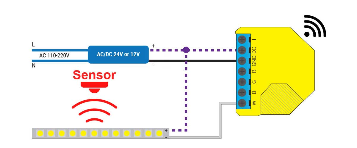 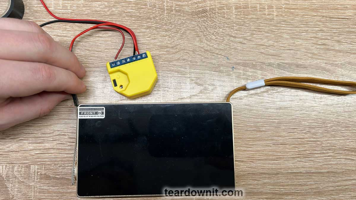 1. Old Shelly native firmware. I found a new old Shelly RGBW2 controller with 2021 firmware in my stock.  Measurements are taken at 25% brightness. The PWM controller is running at 600 Hz. 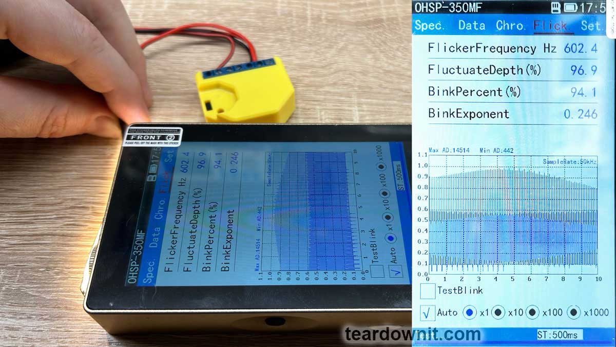 2. New Shelly native firmware (20230913-131259/v1.14.0-gcb84623). The PWM controller operates at 1000 Hz for a brightness of 25%. https://assets-global.website-files.com/6438c93ff266bb9903cab3bc/65f8212d74eaa39564959b06_5.jpg 3. Tasmota firmware. Firmware installation is easily done without wires and additional devices using OTA. Manual: https://github.com/arendst/mgos-to-tasmota However, I couldn't use this script and found many errors mentioned for this device. The solution is found right here: https://github.com/yaourdt/mgos-to-tasmota/issues/102 This is my successful script: RGBW2 must be set to Color mode. You do not need to do anything if the device is already in this mode. The firmware needs to be downloaded from this link: http://deviceIP/ota?url=http://dl.nekohell.eu/mg2tasmota-ShellyRGBW2c.zip Once the WiFi network is configured, you need to use two commands through the Tasmota console (changes will be saved after rebooting or shutting down the device): SetOption68 1 // The device will switch to 4-channel white mode (if you need it)PWMFrequency 2000 // PWM frequency will increase to 2000 Hz Configuration for Tasmota and additional information: https://tasmota.github.io/docs/devices/Shelly-RGBW2/  I set the PWM frequency by a multiple margin (I was just curious). 4000 Hz. 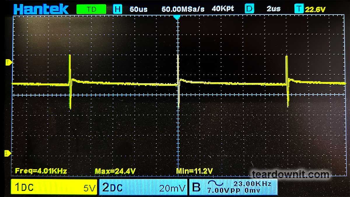 The optical measuring tool showed an incomprehensible picture for me. But this phenomenon is outside the scope of this post, and I will deal with it later. 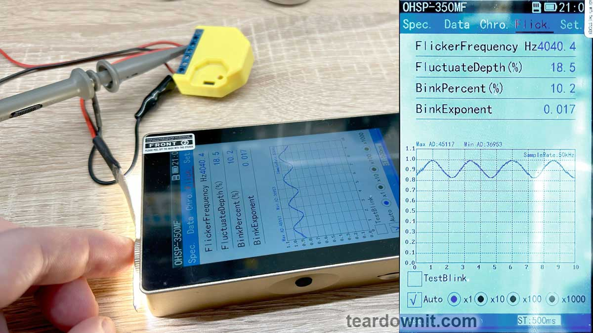 Conclusions. The Shelly device manufacturer can change and does change the PWM frequency in their firmware. I really don't understand their answer about not being able/unwilling to change the PWM frequency to a safe level. I am very grateful to Ciprian for the excellent advice. Thank you, Ciprian! |
| json metadata | {"tags":["pwm"],"image":["https://cdn.steemitimages.com/DQmbJLhoX3yuQwfCprd6vhL79SNeFsNaKz4KtoxeMWaMZH5/image.png","https://cdn.steemitimages.com/DQmWoxC8eQfRThVZR5UrbLEj87LRjM7YoxSEeZUeDDtM2ya/image.png","https://cdn.steemitimages.com/DQmXh9YNhxqFy5Kky43rH6otiGj4jacAzqNgNRDp9J6D6HF/image.png","https://cdn.steemitimages.com/DQmXBNggYysqqCC6AT87TiKeEGP6YoDm5AxaHiMuTbwi8TT/image.png","https://assets-global.website-files.com/6438c93ff266bb9903cab3bc/65f8212d74eaa39564959b06_5.jpg","https://cdn.steemitimages.com/DQmbudo6ht5gL6aqZeQCXra2iCo81LLge3Xev4XZCx3sE3J/image.png","https://cdn.steemitimages.com/DQmaNDm6enjeLjzTFGrEN7JFkKEkPhpBTrNSnuf1J2rtzuy/image.png","https://cdn.steemitimages.com/DQma596QDVNCgQszPQ6q75L5gESBBp3vC4kiH7bgSnqwrY3/image.png"],"links":["https://teardownit.com/posts/shelly-rgbw2-controller-and-shelly-duo-rgbw-bulb-dangerous-light-pulsations","https://esphome.io/components/output/esp8266_pwm.html","https://tasmota.github.io/docs/Commands/#pwmfrequency","https://github.com/arendst/mgos-to-tasmota","https://github.com/yaourdt/mgos-to-tasmota/issues/102","https://tasmota.github.io/docs/devices/Shelly-RGBW2/"],"app":"steemit/0.2","format":"markdown"} |
| parent author | |
| parent permlink | pwm |
| permlink | pwm-frequency-in-shelly-rgbw2-controller |
| title | PWM frequency in Shelly RGBW2 controller |
| Transaction Info | Block #83692523/Trx 6d4b78fb52f082da4f5fb72102a5bea13232899a |
View Raw JSON Data
{
"block": 83692523,
"op": [
"comment",
{
"author": "teardownit",
"body": "I received an interesting email from a reader of my post:\nhttps://teardownit.com/posts/shelly-rgbw2-controller-and-shelly-duo-rgbw-bulb-dangerous-light-pulsations\n\n=====\nAfter having some bloody eyes and reading your article I decided to change the firmware on shelly rgbw2 with ESPHome so I can modify the pwm freq to 1500 Hz like you recommended.\nDon't know if placebo or not but I feel better :) .\n\nI can test only with camera from phone with shutter speed at 1/1500 and no flicker (and sub multiples like 1/500).\nWith PWM freq at 600 Hz I could see flicker on camera at anything above 1/600.\n\nDon't know if this is the same you have tested but I was curious if you can test with a modified Shelly with ESPHome to be able to put higher frequency.\nI also don't know if there is a limit on the maximum frequency (the shelly or the COB LED strip it's dimming ) it will work and if is there any benefit in increasing any further.\n\nThank you for publishing this extensive tests online.\nCiprian\n=====\n\nGreat news!\nI was very interested and read the ESPHome firmware description.\nhttps://esphome.io/components/output/esp8266_pwm.html\nPerfect!\n\nI have not previously used ESPHome, but I have been actively using Tasmota for a long time. In this firmware I also found PWM frequency adjustment:\nhttps://tasmota.github.io/docs/Commands/#pwmfrequency\n\nLet's do the tests!\nThe measurement scheme is simple.\n\n\n\n\n\n\n1. Old Shelly native firmware.\nI found a new old Shelly RGBW2 controller with 2021 firmware in my stock.\n\n\n\nMeasurements are taken at 25% brightness. The PWM controller is running at 600 Hz.\n\n\n\n2. New Shelly native firmware (20230913-131259/v1.14.0-gcb84623).\nThe PWM controller operates at 1000 Hz for a brightness of 25%.\n\nhttps://assets-global.website-files.com/6438c93ff266bb9903cab3bc/65f8212d74eaa39564959b06_5.jpg\n\n3. Tasmota firmware.\nFirmware installation is easily done without wires and additional devices using OTA.\nManual: https://github.com/arendst/mgos-to-tasmota\n\nHowever, I couldn't use this script and found many errors mentioned for this device.\n\nThe solution is found right here:\nhttps://github.com/yaourdt/mgos-to-tasmota/issues/102\n\nThis is my successful script:\n\nRGBW2 must be set to Color mode. You do not need to do anything if the device is already in this mode.\nThe firmware needs to be downloaded from this link:\nhttp://deviceIP/ota?url=http://dl.nekohell.eu/mg2tasmota-ShellyRGBW2c.zip\nOnce the WiFi network is configured, you need to use two commands through the Tasmota console (changes will be saved after rebooting or shutting down the device):\nSetOption68 1 // The device will switch to 4-channel white mode (if you need it)PWMFrequency 2000 // PWM frequency will increase to 2000 Hz\nConfiguration for Tasmota and additional information:\nhttps://tasmota.github.io/docs/devices/Shelly-RGBW2/\n\n\nI set the PWM frequency by a multiple margin (I was just curious). 4000 Hz.\n\n\n\nThe optical measuring tool showed an incomprehensible picture for me. But this phenomenon is outside the scope of this post, and I will deal with it later.\n\n\n\nConclusions.\nThe Shelly device manufacturer can change and does change the PWM frequency in their firmware. I really don't understand their answer about not being able/unwilling to change the PWM frequency to a safe level.\nI am very grateful to Ciprian for the excellent advice. Thank you, Ciprian!",
"json_metadata": "{\"tags\":[\"pwm\"],\"image\":[\"https://cdn.steemitimages.com/DQmbJLhoX3yuQwfCprd6vhL79SNeFsNaKz4KtoxeMWaMZH5/image.png\",\"https://cdn.steemitimages.com/DQmWoxC8eQfRThVZR5UrbLEj87LRjM7YoxSEeZUeDDtM2ya/image.png\",\"https://cdn.steemitimages.com/DQmXh9YNhxqFy5Kky43rH6otiGj4jacAzqNgNRDp9J6D6HF/image.png\",\"https://cdn.steemitimages.com/DQmXBNggYysqqCC6AT87TiKeEGP6YoDm5AxaHiMuTbwi8TT/image.png\",\"https://assets-global.website-files.com/6438c93ff266bb9903cab3bc/65f8212d74eaa39564959b06_5.jpg\",\"https://cdn.steemitimages.com/DQmbudo6ht5gL6aqZeQCXra2iCo81LLge3Xev4XZCx3sE3J/image.png\",\"https://cdn.steemitimages.com/DQmaNDm6enjeLjzTFGrEN7JFkKEkPhpBTrNSnuf1J2rtzuy/image.png\",\"https://cdn.steemitimages.com/DQma596QDVNCgQszPQ6q75L5gESBBp3vC4kiH7bgSnqwrY3/image.png\"],\"links\":[\"https://teardownit.com/posts/shelly-rgbw2-controller-and-shelly-duo-rgbw-bulb-dangerous-light-pulsations\",\"https://esphome.io/components/output/esp8266_pwm.html\",\"https://tasmota.github.io/docs/Commands/#pwmfrequency\",\"https://github.com/arendst/mgos-to-tasmota\",\"https://github.com/yaourdt/mgos-to-tasmota/issues/102\",\"https://tasmota.github.io/docs/devices/Shelly-RGBW2/\"],\"app\":\"steemit/0.2\",\"format\":\"markdown\"}",
"parent_author": "",
"parent_permlink": "pwm",
"permlink": "pwm-frequency-in-shelly-rgbw2-controller",
"title": "PWM frequency in Shelly RGBW2 controller"
}
],
"op_in_trx": 0,
"timestamp": "2024-03-26T21:26:48",
"trx_id": "6d4b78fb52f082da4f5fb72102a5bea13232899a",
"trx_in_block": 11,
"virtual_op": 0
}steemdelegated 10.604 SP to @teardownit2024/03/25 01:56:03
steemdelegated 10.604 SP to @teardownit
2024/03/25 01:56:03
| delegatee | teardownit |
| delegator | steem |
| vesting shares | 17246.573097 VESTS |
| Transaction Info | Block #83640482/Trx 418f3b47a9eb3bc447b708e00fa9e81dd3968e01 |
View Raw JSON Data
{
  "block": 83640482,
  "op": [
    "delegate_vesting_shares",
    {
      "delegatee": "teardownit",
      "delegator": "steem",
      "vesting_shares": "17246.573097 VESTS"
    }
  ],
  "op_in_trx": 0,
  "timestamp": "2024-03-25T01:56:03",
  "trx_id": "418f3b47a9eb3bc447b708e00fa9e81dd3968e01",
  "trx_in_block": 4,
  "virtual_op": 0
}bluesnipersent 0.010 STEEM to @teardownit- "Hello. Good to see you on Steem. To maximize your rewards, publish your post also on Hive ( hive.blog ) and Blurt ( blurt.blog ) blockchains. Use upvu, jsup or ctime and get instant upvotes"2024/03/24 08:07:00
bluesnipersent 0.010 STEEM to @teardownit- "Hello. Good to see you on Steem. To maximize your rewards, publish your post also on Hive ( hive.blog ) and Blurt ( blurt.blog ) blockchains. Use upvu, jsup or ctime and get instant upvotes"
2024/03/24 08:07:00
| amount | 0.010 STEEM |
| from | bluesniper |
| memo | Hello. Good to see you on Steem. To maximize your rewards, publish your post also on Hive ( hive.blog ) and Blurt ( blurt.blog ) blockchains. Use upvu, jsup or ctime and get instant upvotes |
| to | teardownit |
| Transaction Info | Block #83619184/Trx 15e75777a50dfc8bafdc9a836e1e99b05b69c4c4 |
View Raw JSON Data
{
  "block": 83619184,
  "op": [
    "transfer",
    {
      "amount": "0.010 STEEM",
      "from": "bluesniper",
      "memo": "Hello. Good to see you on Steem. To maximize your rewards, publish your post also on Hive ( hive.blog ) and Blurt ( blurt.blog ) blockchains. Use upvu, jsup or ctime and get instant upvotes",
      "to": "teardownit"
    }
  ],
  "op_in_trx": 0,
  "timestamp": "2024-03-24T08:07:00",
  "trx_id": "15e75777a50dfc8bafdc9a836e1e99b05b69c4c4",
  "trx_in_block": 7,
  "virtual_op": 0
}bluesniperupvoted (100.00%) @teardownit / finding-water-damage-in-a-cable-using-a-reflectometer2024/03/24 08:06:39
bluesniperupvoted (100.00%) @teardownit / finding-water-damage-in-a-cable-using-a-reflectometer
2024/03/24 08:06:39
| author | teardownit |
| permlink | finding-water-damage-in-a-cable-using-a-reflectometer |
| voter | bluesniper |
| weight | 10000 (100.00%) |
| Transaction Info | Block #83619177/Trx bea69da9a5485448d0f6e0c1169b34c235e4c163 |
View Raw JSON Data
{
  "block": 83619177,
  "op": [
    "vote",
    {
      "author": "teardownit",
      "permlink": "finding-water-damage-in-a-cable-using-a-reflectometer",
      "voter": "bluesniper",
      "weight": 10000
    }
  ],
  "op_in_trx": 0,
  "timestamp": "2024-03-24T08:06:39",
  "trx_id": "bea69da9a5485448d0f6e0c1169b34c235e4c163",
  "trx_in_block": 0,
  "virtual_op": 0
}teardownitpublished a new post: finding-water-damage-in-a-cable-using-a-reflectometer2024/03/24 08:01:03
teardownitpublished a new post: finding-water-damage-in-a-cable-using-a-reflectometer
2024/03/24 08:01:03
| author | teardownit |
| body | Despite all the hard efforts to keep IT cables dry, water remains the most likely cause of cable failure. Water introduction into the cable leads to various types of damage, often resulting in a high-resistance short circuit. Signs of cable water ingress change over time. Usually, the first symptom is the appearance of noise on the line. Interference occurs due to the flow of microcurrents between conductors. Suppose the service personnel do not take any measures. The problem may grow in that case, so communication will be blocked entirely. Cables with some water inside them can be categorized into two types: wet and waterlogged. Most of the time, the cable is simply soaked. In cables with filler, water can accumulate in existing voids and in overhead cables in sagging sections. In warm weather, it evaporates, and in cold weather, it condenses back again. As a result, the copper wires corrode, increasing resistance and causing poor cable performance. Water ingress occurs when water penetrates the cable through a damaged jacket. In this case, the impact may come from groundwater, melting snow, precipitation, etc. A cable submerged in water may work normally until it inevitably does not. SEARCHING FOR WATER INGRESS SPOTS Water impact is found when the reflectometer detects a change in the resistance of the pair being tested due to a change in its capacitance. In addition, a good indicator can be the pulse propagation speed, which directly depends on the characteristics of the cable. Water in the cable "slows down" the signal. In the waterlogged section, the electrical signal's propagation speed can change every other inch. As a result, measuring the actual length of the entire cable and its waterlogged section is much more challenging since the reflectometer measures time intervals. (The bridge meter will indicate that the cable length is longer than the actual length.) Water significantly increases the capacitance of the waterlogged section of the cable, so it will not be possible to find the correct propagation coefficient value. To reliably measure the cable length, one usually measures the length of a dry section, either on one or both sides. If the total length of the cable is known, subtract the lengths of the dry sections from it. Very often, the starting point of the waterlogged segment is too close to the reflectometer connection point. In this case, the device will not detect the presence of water. Therefore, the cable must be checked from both sides. Some OTDRs have a "marker" function to measure the distance between two points, eliminating the need to measure dry sections on both sides of the cable and making it easier to determine the length of a waterlogged section. https://assets-global.website-files.com/6438c93ff266bb9903cab3bc/65f2b623f48656f256584d2a_Pic-1.jpg The figure shows that L2 = Lcable – (L1 + L3), where L2 is the known cable length and L1 and L3 are dry sections. Water ingress affects the operation of multiple cable pairs. When testing a disconnected or inactive pair, there is a possibility that some voltage may be induced by neighboring active pairs, which is why most testing methods, such as using bridge meters, lead to distorted results. In such a situation, a reflectometer is the only device that will allow one to find the water damage point. https://assets-global.website-files.com/6438c93ff266bb9903cab3bc/65f2b633971cf823dede1a04_Pic-2.jpg The classic reflectogram of a waterlogged cable has three key features. The first is a decline in the reflectogram (reflected pulse of negative polarity) in the place where the section of the waterlogged cable starts. The second is a waterlogged segment of the cable, usually having a slightly curved characteristic with "noise" (this is not noise per se, but simply an impedance unevenness that causes a characteristic distortion to appear on that section of the cable). Finally, the third is the rise of the reflectogram at the end of the waterlogged section of the cable (the reflected pulse of positive polarity). The reference reflectogram in the figure illustrates the ideal case. It is important to emphasize that the water in the cable significantly weakens the reflectometer signal. If the waterlogged segment is too long, then the farther end of it can be indiscernible on the OTDR's display. https://assets-global.website-files.com/6438c93ff266bb9903cab3bc/65f2b64778239f4884edf590_Pic-3.jpg On a real reflectogram of a cable with water in the coupling, a signal is reflected both from the place of the cable coupling and the waterlogged section of the cable. It is quite difficult to notice initially, but increasing the gain level will make the reflectogram more straightforward. https://assets-global.website-files.com/6438c93ff266bb9903cab3bc/65f2b65d64497df440d71f1b_Pic-4.jpg After increasing the gain level, it is much easier to see the classic decline in the reflectogram after the cable coupling (at a distance of approximately 2500 feet) and the uneven reflectogram for the waterlogged section of the cable (at a distance of about 2500–3000 feet). The reflectogram line goes up at the place where the waterlogged section of the cable ends (at a distance of approximately 3300 feet). In addition, the end of the cable can be clearly defined at 6500 feet. TROUBLESHOOTING A WATERLOGGED CABLE SECTION One of the most challenging tasks associated with troubleshooting using an OTDR is identifying faults in a water-damaged cable section. The reflectogram will indicate water ingress, but the locations of various faults are usually masked by distortions caused by the water in the cable. The procedure for searching for damage in waterlogged cable sections using a reflectometer is shown above. It allows one to see the advantages of the differential measurement method in real-time. https://assets-global.website-files.com/6438c93ff266bb9903cab3bc/65f2b66fd2a942ddb7cda232_Pic-5.jpg The reflectometer display will display the difference between the characteristics of the "good" and the pair being tested. Both pass through the same waterlogged section of the cable, so the water will not affect the final reflectogram; only the differences between the two pairs will remain on it. Once the display shows the location of the damage, one can measure the distance to it. So, suppose there is a suspicion that water has gotten inside the cable, first of all. In that case, it is necessary to determine the location of the affected segment. The role of a reflectometer in quickly localizing where water enters a cable cannot be overestimated. |
| json metadata | {"tags":["meanwell"],"image":["https://assets-global.website-files.com/6438c93ff266bb9903cab3bc/65f2b623f48656f256584d2a_Pic-1.jpg","https://assets-global.website-files.com/6438c93ff266bb9903cab3bc/65f2b633971cf823dede1a04_Pic-2.jpg","https://assets-global.website-files.com/6438c93ff266bb9903cab3bc/65f2b64778239f4884edf590_Pic-3.jpg","https://assets-global.website-files.com/6438c93ff266bb9903cab3bc/65f2b65d64497df440d71f1b_Pic-4.jpg","https://assets-global.website-files.com/6438c93ff266bb9903cab3bc/65f2b66fd2a942ddb7cda232_Pic-5.jpg"],"app":"steemit/0.2","format":"markdown"} |
| parent author | |
| parent permlink | meanwell |
| permlink | finding-water-damage-in-a-cable-using-a-reflectometer |
| title | Finding water damage in a cable using a reflectometer |
| Transaction Info | Block #83619065/Trx b6062572bdbe96ded67cdb2f642ec1c069a60fcf |
View Raw JSON Data
{
  "block": 83619065,
  "op": [
    "comment",
    {
      "author": "teardownit",
      "body": "Despite all the hard efforts to keep IT cables dry, water remains the most likely cause of cable failure. Water introduction into the cable leads to various types of damage, often resulting in a high-resistance short circuit.\n\nSigns of cable water ingress change over time. Usually, the first symptom is the appearance of noise on the line. Interference occurs due to the flow of microcurrents between conductors. Suppose the service personnel do not take any measures. The problem may grow in that case, so communication will be blocked entirely. Cables with some water inside them can be categorized into two types: wet and waterlogged. Most of the time, the cable is simply soaked. In cables with filler, water can accumulate in existing voids and in overhead cables in sagging sections. In warm weather, it evaporates, and in cold weather, it condenses back again. As a result, the copper wires corrode, increasing resistance and causing poor cable performance.\n\nWater ingress occurs when water penetrates the cable through a damaged jacket. In this case, the impact may come from groundwater, melting snow, precipitation, etc. A cable submerged in water may work normally until it inevitably does not.\n\nSEARCHING FOR WATER INGRESS SPOTS\nWater impact is found when the reflectometer detects a change in the resistance of the pair being tested due to a change in its capacitance. In addition, a good indicator can be the pulse propagation speed, which directly depends on the characteristics of the cable.\n\nWater in the cable \"slows down\" the signal. In the waterlogged section, the electrical signal's propagation speed can change every other inch. As a result, measuring the actual length of the entire cable and its waterlogged section is much more challenging since the reflectometer measures time intervals. (The bridge meter will indicate that the cable length is longer than the actual length.) Water significantly increases the capacitance of the waterlogged section of the cable, so it will not be possible to find the correct propagation coefficient value. To reliably measure the cable length, one usually measures the length of a dry section, either on one or both sides. If the total length of the cable is known, subtract the lengths of the dry sections from it. Very often, the starting point of the waterlogged segment is too close to the reflectometer connection point. In this case, the device will not detect the presence of water. Therefore, the cable must be checked from both sides.\n\nSome OTDRs have a \"marker\" function to measure the distance between two points, eliminating the need to measure dry sections on both sides of the cable and making it easier to determine the length of a waterlogged section.\n\nhttps://assets-global.website-files.com/6438c93ff266bb9903cab3bc/65f2b623f48656f256584d2a_Pic-1.jpg\nThe figure shows that L2 = Lcable – (L1 + L3), where L2 is the known cable length and L1 and L3 are dry sections.\n\nWater ingress affects the operation of multiple cable pairs. When testing a disconnected or inactive pair, there is a possibility that some voltage may be induced by neighboring active pairs, which is why most testing methods, such as using bridge meters, lead to distorted results. In such a situation, a reflectometer is the only device that will allow one to find the water damage point.\n\nhttps://assets-global.website-files.com/6438c93ff266bb9903cab3bc/65f2b633971cf823dede1a04_Pic-2.jpg\n\nThe classic reflectogram of a waterlogged cable has three key features. The first is a decline in the reflectogram (reflected pulse of negative polarity) in the place where the section of the waterlogged cable starts. The second is a waterlogged segment of the cable, usually having a slightly curved characteristic with \"noise\" (this is not noise per se, but simply an impedance unevenness that causes a characteristic distortion to appear on that section of the cable). Finally, the third is the rise of the reflectogram at the end of the waterlogged section of the cable (the reflected pulse of positive polarity). The reference reflectogram in the figure illustrates the ideal case.\n\nIt is important to emphasize that the water in the cable significantly weakens the reflectometer signal. If the waterlogged segment is too long, then the farther end of it can be indiscernible on the OTDR's display. \n\nhttps://assets-global.website-files.com/6438c93ff266bb9903cab3bc/65f2b64778239f4884edf590_Pic-3.jpg\n\nOn a real reflectogram of a cable with water in the coupling, a signal is reflected both from the place of the cable coupling and the waterlogged section of the cable. It is quite difficult to notice initially, but increasing the gain level will make the reflectogram more straightforward.\n\nhttps://assets-global.website-files.com/6438c93ff266bb9903cab3bc/65f2b65d64497df440d71f1b_Pic-4.jpg\n\nAfter increasing the gain level, it is much easier to see the classic decline in the reflectogram after the cable coupling (at a distance of approximately 2500 feet) and the uneven reflectogram for the waterlogged section of the cable (at a distance of about 2500–3000 feet). The reflectogram line goes up at the place where the waterlogged section of the cable ends (at a distance of approximately 3300 feet). In addition, the end of the cable can be clearly defined at 6500 feet.\n\nTROUBLESHOOTING A WATERLOGGED CABLE SECTION\nOne of the most challenging tasks associated with troubleshooting using an OTDR is identifying faults in a water-damaged cable section. The reflectogram will indicate water ingress, but the locations of various faults are usually masked by distortions caused by the water in the cable.\n\nThe procedure for searching for damage in waterlogged cable sections using a reflectometer is shown above. It allows one to see the advantages of the differential measurement method in real-time.\n\nhttps://assets-global.website-files.com/6438c93ff266bb9903cab3bc/65f2b66fd2a942ddb7cda232_Pic-5.jpg\n\nThe reflectometer display will display the difference between the characteristics of the \"good\" and the pair being tested. Both pass through the same waterlogged section of the cable, so the water will not affect the final reflectogram; only the differences between the two pairs will remain on it. Once the display shows the location of the damage, one can measure the distance to it.\n\nSo, suppose there is a suspicion that water has gotten inside the cable, first of all. In that case, it is necessary to determine the location of the affected segment. The role of a reflectometer in quickly localizing where water enters a cable cannot be overestimated.",
      "json_metadata": "{\"tags\":[\"meanwell\"],\"image\":[\"https://assets-global.website-files.com/6438c93ff266bb9903cab3bc/65f2b623f48656f256584d2a_Pic-1.jpg\",\"https://assets-global.website-files.com/6438c93ff266bb9903cab3bc/65f2b633971cf823dede1a04_Pic-2.jpg\",\"https://assets-global.website-files.com/6438c93ff266bb9903cab3bc/65f2b64778239f4884edf590_Pic-3.jpg\",\"https://assets-global.website-files.com/6438c93ff266bb9903cab3bc/65f2b65d64497df440d71f1b_Pic-4.jpg\",\"https://assets-global.website-files.com/6438c93ff266bb9903cab3bc/65f2b66fd2a942ddb7cda232_Pic-5.jpg\"],\"app\":\"steemit/0.2\",\"format\":\"markdown\"}",
      "parent_author": "",
      "parent_permlink": "meanwell",
      "permlink": "finding-water-damage-in-a-cable-using-a-reflectometer",
      "title": "Finding water damage in a cable using a reflectometer"
    }
  ],
  "op_in_trx": 0,
  "timestamp": "2024-03-24T08:01:03",
  "trx_id": "b6062572bdbe96ded67cdb2f642ec1c069a60fcf",
  "trx_in_block": 1,
  "virtual_op": 0
}teardownitdeleted a comment or post2024/03/19 07:34:18
teardownitdeleted a comment or post
2024/03/19 07:34:18
| author | teardownit |
| permlink | review-teardown-and-testing-of-rsp-320-24-mean-well-power-supply |
| Transaction Info | Block #83475048/Trx b5b23f8d468c570f7e07492fa3e6fcce709aac9f |
View Raw JSON Data
{
  "block": 83475048,
  "op": [
    "delete_comment",
    {
      "author": "teardownit",
      "permlink": "review-teardown-and-testing-of-rsp-320-24-mean-well-power-supply"
    }
  ],
  "op_in_trx": 0,
  "timestamp": "2024-03-19T07:34:18",
  "trx_id": "b5b23f8d468c570f7e07492fa3e6fcce709aac9f",
  "trx_in_block": 5,
  "virtual_op": 0
}teardownitpublished a new post: review-teardown-and-testing-of-rsp-320-24-mean-well-power-supply2024/03/19 07:34:00
teardownitpublished a new post: review-teardown-and-testing-of-rsp-320-24-mean-well-power-supply
2024/03/19 07:34:00
| author | teardownit |
| body | 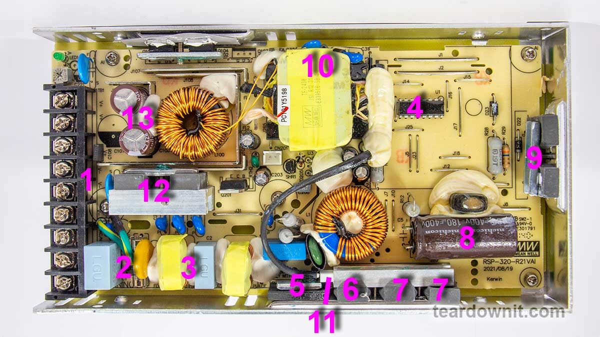 The RSP-320-24 is a 24-volt power supply with a maximum current of 13.4 amps. The supported mains voltage is from 100 to 240 volts without an additional switch. The supply measures 8.5 × 4.5 × 1¼ inches (215 × 115 × 30 millimeters), made on a printed circuit board fixed to the base's case. The top cover is perforated at the back near the connection terminals and on the front, where the cooling fan is installed. The fan starts spinning even if there's no electrical load. As the load increases, the fan speeds up, following the load current value. The fan sucks in the air and pushes it through the internal case volume to the perforated holes, including those on the side walls. The input and output circuits are connected to a standard screw terminal block (1), from right to left: 3 terminals for the input line, neutral and ground wires, and 3 in parallel for common and +24V output. The input voltage from the terminals goes to the fuse (2), then to the pulse limiter (varistor), followed by the RF interference filter (3), and finally to the diode bridge (5). Next comes the active PFC, controlled by the PFC+PWM controller FAN4800 (4). Indeed, with a 234-volt AC power input, we get a rectified voltage on the storage capacitor (8) of 377 volts, approximately 47 volts more than without PFC Boost. The small voltage reserve is confusing since the capacitor installed is rated for 180 uF and 400 volts. All that's left is to rely on Nichicon's quality control. The power part of the PFC is made of two parallel MOSFETs, IPP60R280P6 (7) and on an ultrafast diode 8A 600V STTH8S06D (6). The temperature sensor (11) is mounted above the PFC elements. The output voltage from the PFC is supplied to the two-transistor forward converter; the transistors are IPP60R280P6 (9) and are controlled by the same FAN4800 controller. The transformer (10) converter voltage is rectified and supplied to the LC filter. The output rectifier comprises eight diodes connected in two parallel groups (12). Total output capacitance: 2 pieces of 1000uF, 35V, designed for operating temperatures up to 220°F (105°C) (13). The output high-current circuits are reinforced with tinned copper busbars. The control signal from the high-voltage side to the low-voltage side is transmitted through transistor optocouplers (there are two of them in the photo above the transformer hidden under a blob of the compound). One optocoupler is the primary regulation channel, and the second forms a backup channel for overvoltage protection, OVP. 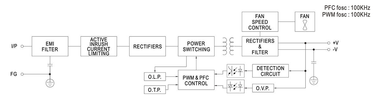 The block diagram in the datasheet shows the "Active Inrush Current Limiting" node. Still, we could not find components on the board that could perform such a role. Still, the inrush current limitation element is present, marked as RTH1 on the board, and installed near the boost inductor PFC; most likely, this is an ordinary NTC. The high-voltage part of the board, starting with the capacitor (8) and ending with the transformer leads (10), is coated on the high-voltage side with a protective composite, presumably epoxy-based, which further increases electrical safety. There is additional insulation and a thin sheet of fiberglass between the aluminum case and the board (solder side). The overall build quality is good. >Test conditions Most tests use metering circuit #1 (see appendices) at 80°F (27°C), 70% relative humidity, and 29.8 inHg pressure. The measurements were performed without preheating the power supply with a short-term load unless mentioned otherwise. The following values were used to determine the load level: Test conditions Most tests use metering circuit #1 (see appendices) at 80°F (27°C), 70% relative humidity, and 29.8 inHg pressure. The measurements were performed without preheating the power supply with a short-term load unless mentioned otherwise. The following values were used to determine the load level: 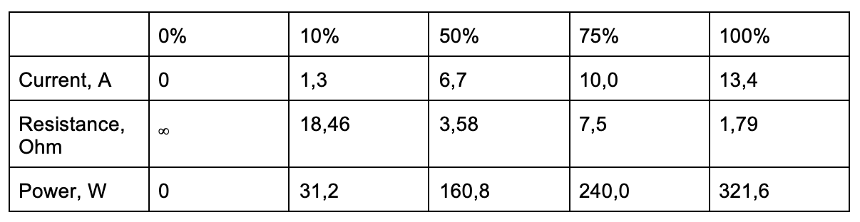 Output voltage under a constant load  The high stability of the output voltage should be noted. >Power-on parameters Powering on at 100% load The power supply is turned off at least 5 minutes before the test, with a 100% load connected. The oscillogram of switching to a 100% load is shown below (channel 1 is the output voltage, and channel 2 is the current consumption from the grid):  The picture shows three distinguishable phases of the power-on process: The pulse of the input current charging the input capacitors when connected to the grid has an amplitude of about 2 A and a duration north of the mains voltage period. Waiting for the power supply control circuit to start for about 300 ms. (Output Voltage Rise Time) Starting the converter, increasing the output voltage, and entering the operating mode takes 8 ms. (Turn On Delay Time) The entire process of entering the operating mode from the moment of powering on is 315 ms. (Output Voltage Overshoot) The switching process is aperiodic; there is no overshoot. >Powering on at 0% load The power supply is turned off at least 5 minutes before the test, with a 100% load connected. Then, the load is disconnected, and the power supply is switched on. The oscillogram of switching to a 0% load is shown below:  The picture shows three distinguishable phases of the power-on process: The pulse of the input current charging the input capacitors when connected to the grid has an amplitude of about 2.2 A and a duration slightly longer than one mains period. Waiting for the power supply control circuit to start for about 300 ms. (Output Voltage Rise Time) Starting the converter, increasing the output voltage, and entering the operating mode takes 7 ms. (Turn On Delay Time) The entire process of entering the operating mode from the moment of powering on is 320 ms. (Output Voltage Overshoot) The switching process is aperiodic; there is no overshoot. >Power-off parameters The power supply was turned off at 100% load, and the input voltage was nominal at the moment of powering off. The oscillogram of the shutdown process is shown below:  The picture shows two phases of the shutdown process: (Shutdown Hold-Up Time) The power supply continues to operate due to the input capacitors holding charge until the voltage across them drops to a certain critical level, at which maintaining the output voltage at the nominal level becomes impossible. The phase takes 14 ms. (Output Voltage Fall Time) Reduction of the output voltage, stopping voltage conversion, and accelerating the voltage drop takes 18 ms. (Output Voltage Undershoot) The shutdown process is aperiodic; there is no overshoot. Right before shutdown, the current waveform at 100% load is close to sinusoidal with an amplitude of 4.22 A. >Ripple output voltage 100% load At 100% load, the low-frequency ripple is approximately 3 mV. 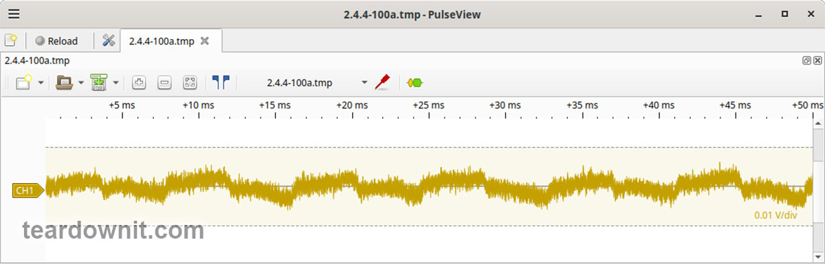 At 100% load, the ripple at the converter frequency is approximately 50 mVp-p, and the noise is 120 mVp-p. 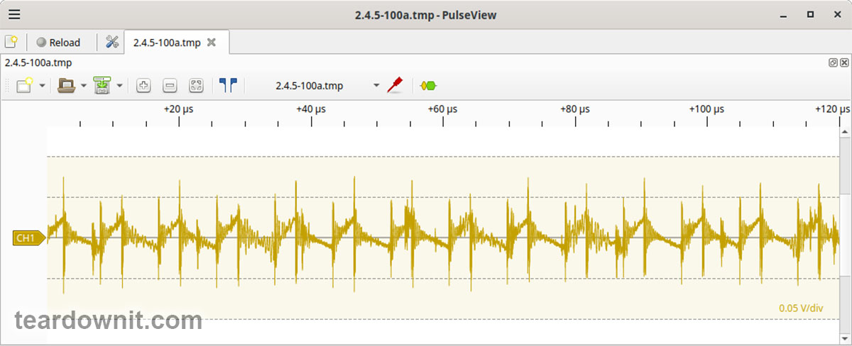 75% load At 75% load, the low-frequency ripple is approximately 3 mV. 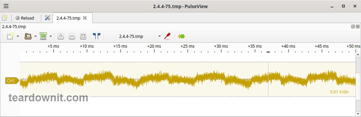 At 75% load, the ripple at the converter frequency is approximately 40 mVp-p, and the noise is 120 mVp-p. 50% load At a 50% load, the low-frequency ripple is approximately 3 mV. 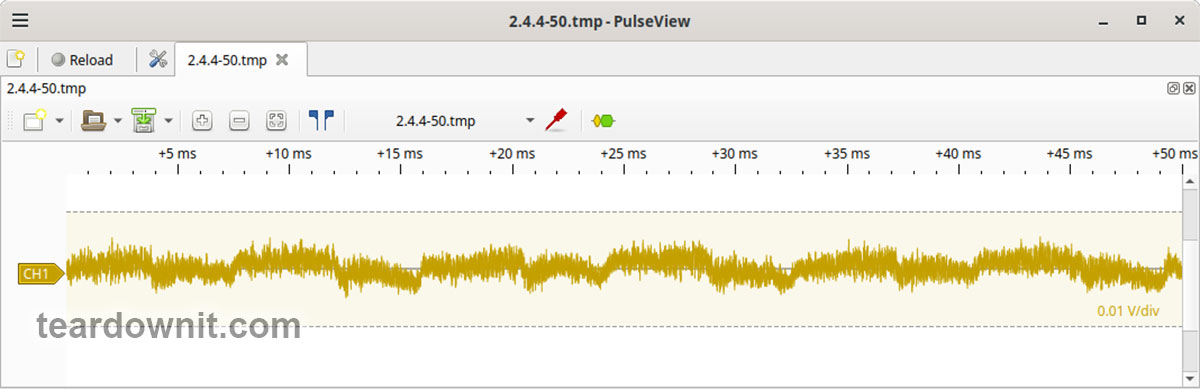 At 50% load, the ripple at the converter frequency is approximately 30 mVp-p, and the noise is 70 mVp-p.  10% load At 10% load, the low-frequency ripple is approximately 2 mV.  At a 10% load, the ripple at the converter frequency is approximately 20 mVp-p, and the noise is 90 mVp-p.  >0% load No-load current consumption measured with a multimeter: 53.5 mA. (Power Consumption) The first assumption of excessive standby power draw of more than 6.5 watts is wrong since the current in this mode is predominantly reactive. Indeed, the input filter in the circuit contains two capacitors with a combined capacitance of 1.5 μF. Measuring the exact active power consumption at a 0% load with a basic set of instruments (oscilloscope, multimeter, etc.) is impossible. At 10% load, the low-frequency ripple is approximately 2 mV.  At 10% load, ripples at the converter frequency are masked by the 90 mVp-p noise.  >Dynamic characteristics TA mode with periodic switching between 50% and 100% load was used to evaluate the dynamic characteristics. The process oscillogram is shown below: 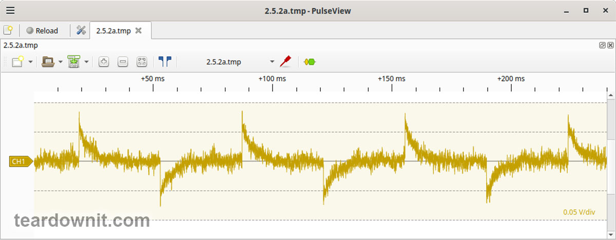 >Input circuit safety assessment (Input discharge) Safety assessment is based on the discharge time constant of the input circuits when disconnected from the grid; the value is 0.26 s. This means that when operating on a 120 V input voltage, the time required to discharge the input circuits to safe values (<42 V) will be 0.41 s:  Important: The result is valid for this particular power supply unit; it was obtained for testing purposes and should not be taken as a safety guarantee. 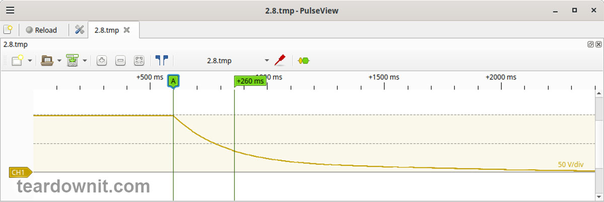 The leakage current at the ground pin is less than 10 µA. Thermal conditions When operating with no load connected, no component overheating had been noticed. Thermograms were captured at three power levels: 80, 90, and 100%, fully assembled and with the lid removed. Thermal images show that the most loaded element of the block is the input diode bridge, and its heating seriously stands out against the background of all the other components. Unfortunately, already at 80% load, the diode bridge heats up to an unacceptable level of 259°F (126°C), which is dangerous for long-term operation. >80% load 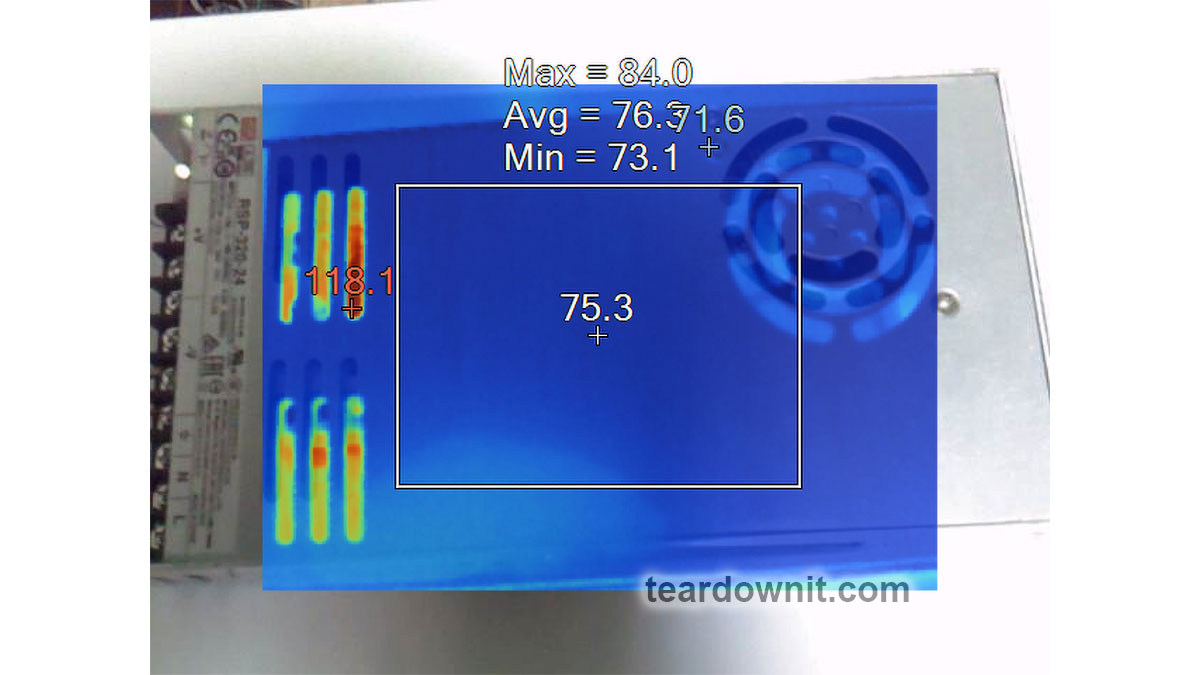 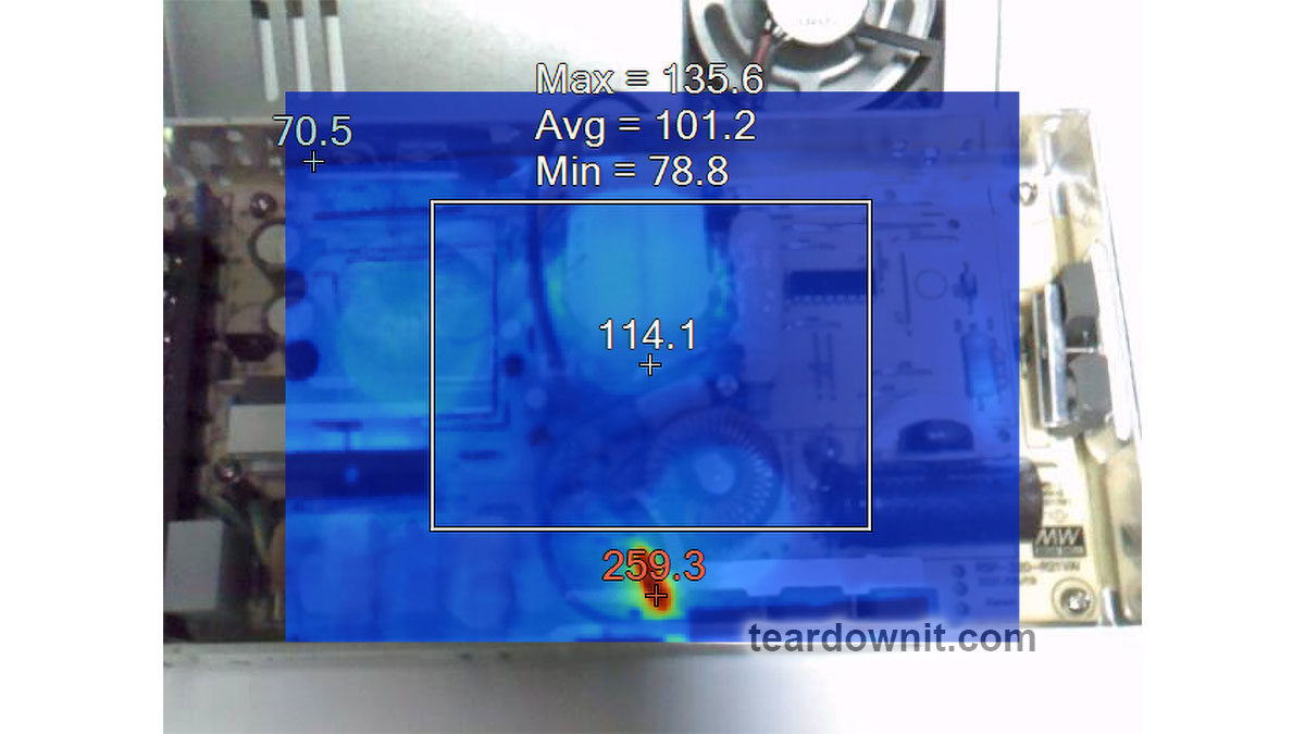 >90% load 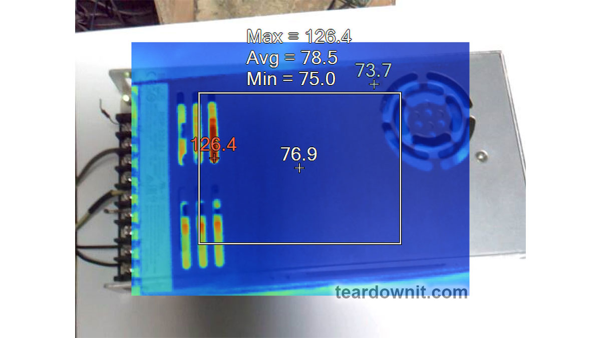 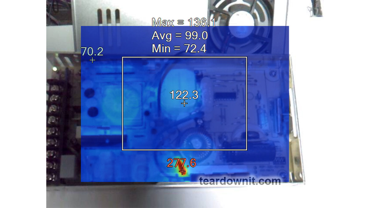 >100% load 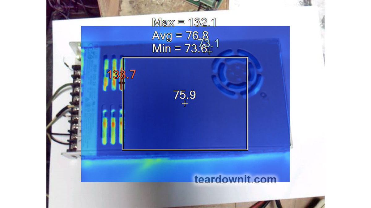 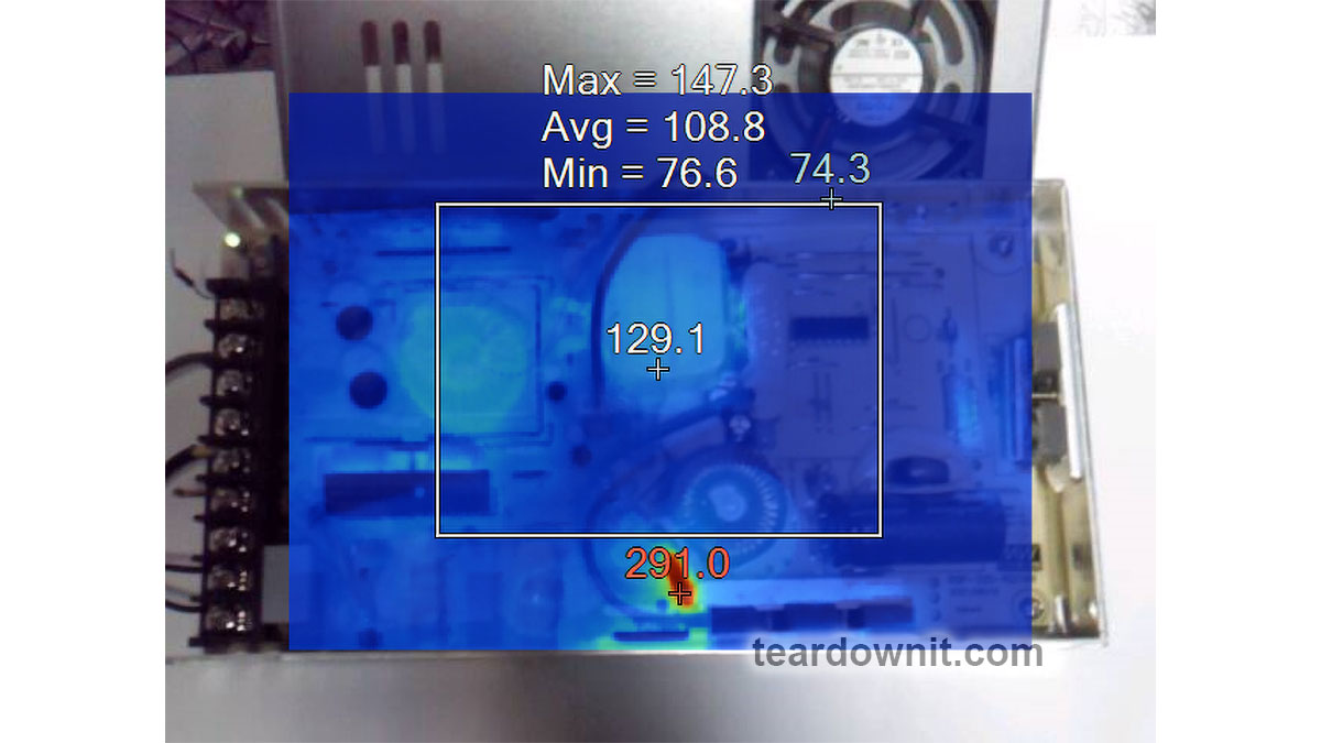 >Conclusions Overall, the RSP-320-24 is well-built: this power supply has good dynamic characteristics, low noise, and ripple, good accuracy in maintaining the output voltage, and is well put together. The load should be limited to 70–80% of the nominal for long-term operation. Important: The results are valid for this particular power supply unit; they were obtained for testing purposes and should not be used to evaluate all the units of the same type. |
| json metadata | {"tags":["teardown"],"image":["https://cdn.steemitimages.com/DQmSM2CASzPANdaNjCYvfXfaGSRCciY67kbLBccneFSdUEn/image.png","https://cdn.steemitimages.com/DQmPEgUc3s4Xhv6KZ1yeik7BabyfAmCyFQeqEFXsu7jqw1W/image.png","https://cdn.steemitimages.com/DQmUC8mBytBStsLEaaWDDyNM5iv7H6N9stry7khcFMoSh1m/image.png","https://cdn.steemitimages.com/DQmevwGhjVKZ8gKim5Kcg3vt9qsjqPr7PHmiFtvBHdY5oLB/image.png","https://cdn.steemitimages.com/DQmTjRgXGfPa8q38eZvB4y2WcYtKCeUVtsYjDn5URX7zyS5/image.png","https://cdn.steemitimages.com/DQmNmE37hsY3fkqhxpFRb4oMq2VLPiKYNdCr46ux8HLqVG9/image.png","https://cdn.steemitimages.com/DQmZKz689HVJk1ttRx7pZWcb5jczR1nQyhwzH9qb4YxiG8F/image.png","https://cdn.steemitimages.com/DQmd2pzQntcgQURKcmyK11cRtX4AqxfHUkmoggJhMrmA9eR/image.png","https://cdn.steemitimages.com/DQmVHoiY5JBR74ha17364isAdWmjjto6TRCvow3A911iXgK/image.png","https://cdn.steemitimages.com/DQmeBru2zSCLATVS4cuFVdvmHzogKx4dkfLRzJRqpGYirKD/image.png","https://cdn.steemitimages.com/DQmSQ5XmDNkhPnU7GFD3nTFmFmodpnT6mscmXMHVwAabC1d/image.png","https://cdn.steemitimages.com/DQmdCcZuFqH5SkQi19eHinfhpMiTgHVQYwUKAEgz8Nxhhj6/image.png","https://cdn.steemitimages.com/DQmQkEd7caxJG61gxLLoX2jq7thD1FPvMxpoNENNHXRz4kc/image.png","https://cdn.steemitimages.com/DQmRvteFmiVRD9qnkb1agZbydVXt3zc8anfGXKGieTPfHtb/image.png","https://cdn.steemitimages.com/DQma7u9Wv17kvwGkqQ51eZaJbRYB7GUeWZp241HRdehAZWT/image.png","https://cdn.steemitimages.com/DQmNfktpV2T7eneZbjuVgLSUJWiZWi9JkbjLLUV38a8LdwE/image.png","https://cdn.steemitimages.com/DQmV8nGT1htrJfErRiBRtbLxDLZizoRm4BC1FF9KhkftzZq/image.png","https://cdn.steemitimages.com/DQmSmd17A4tzmtC5WRZmu5oCTq6ktvHthtnm8LhqNAuYkCi/image.png","https://cdn.steemitimages.com/DQmXFYDFW9GvacbLACp8yv7GUsQj7WYZKzGCCmc63EBaQ2J/image.png","https://cdn.steemitimages.com/DQmUYKRdRuTUjcvKWtskNxTwigN8278f8E34AG8w8bLocSF/image.png","https://cdn.steemitimages.com/DQmScwAtQrbYBpayWzo2TJwUdgwkqCzQGyr7zWZDCsmPXwg/image.png","https://cdn.steemitimages.com/DQmbV9S5Pn5Kd4hPH9r3qPCtFDVJvHAT8RhMfGeT3Fewz5W/image.png","https://cdn.steemitimages.com/DQmTqxmQ3o1uoygP4usgRrD7ttJqeNFtsBnWEaN7tf6JqCB/image.png","https://cdn.steemitimages.com/DQmSMeNKfWULopERY1Y8EjXyZFox4ftEfFeBMniX44KbenE/image.png","https://cdn.steemitimages.com/DQmTPEQqgXNeWLnqtbLqNn8iv1i6JDJxBytpTirhzxXbnKh/image.png"],"app":"steemit/0.2","format":"markdown"} |
| parent author | |
| parent permlink | teardown |
| permlink | review-teardown-and-testing-of-rsp-320-24-mean-well-power-supply |
| title | Review, teardown, and testing of RSP-320-24 Mean Well power supply |
| Transaction Info | Block #83475042/Trx 517595fc4bcd2c88b6987a04e359189bfab56237 |
View Raw JSON Data
{
"block": 83475042,
"op": [
"comment",
{
"author": "teardownit",
"body": "\n\nThe RSP-320-24 is a 24-volt power supply with a maximum current of 13.4 amps. The supported mains voltage is from 100 to 240 volts without an additional switch. The supply measures 8.5 × 4.5 × 1¼ inches (215 × 115 × 30 millimeters), made on a printed circuit board fixed to the base's case. The top cover is perforated at the back near the connection terminals and on the front, where the cooling fan is installed. The fan starts spinning even if there's no electrical load. As the load increases, the fan speeds up, following the load current value. The fan sucks in the air and pushes it through the internal case volume to the perforated holes, including those on the side walls.\n\nThe input and output circuits are connected to a standard screw terminal block (1), from right to left: 3 terminals for the input line, neutral and ground wires, and 3 in parallel for common and +24V output. The input voltage from the terminals goes to the fuse (2), then to the pulse limiter (varistor), followed by the RF interference filter (3), and finally to the diode bridge (5). Next comes the active PFC, controlled by the PFC+PWM controller FAN4800 (4). Indeed, with a 234-volt AC power input, we get a rectified voltage on the storage capacitor (8) of 377 volts, approximately 47 volts more than without PFC Boost. The small voltage reserve is confusing since the capacitor installed is rated for 180 uF and 400 volts. All that's left is to rely on Nichicon's quality control.\n\nThe power part of the PFC is made of two parallel MOSFETs, IPP60R280P6 (7) and on an ultrafast diode 8A 600V STTH8S06D (6). The temperature sensor (11) is mounted above the PFC elements. The output voltage from the PFC is supplied to the two-transistor forward converter; the transistors are IPP60R280P6 (9) and are controlled by the same FAN4800 controller. The transformer (10) converter voltage is rectified and supplied to the LC filter. The output rectifier comprises eight diodes connected in two parallel groups (12). Total output capacitance: 2 pieces of 1000uF, 35V, designed for operating temperatures up to 220°F (105°C) (13). The output high-current circuits are reinforced with tinned copper busbars.\n\nThe control signal from the high-voltage side to the low-voltage side is transmitted through transistor optocouplers (there are two of them in the photo above the transformer hidden under a blob of the compound). One optocoupler is the primary regulation channel, and the second forms a backup channel for overvoltage protection, OVP.\n\n\n\n\nThe block diagram in the datasheet shows the \"Active Inrush Current Limiting\" node. Still, we could not find components on the board that could perform such a role. Still, the inrush current limitation element is present, marked as RTH1 on the board, and installed near the boost inductor PFC; most likely, this is an ordinary NTC.\n\nThe high-voltage part of the board, starting with the capacitor (8) and ending with the transformer leads (10), is coated on the high-voltage side with a protective composite, presumably epoxy-based, which further increases electrical safety.\n\nThere is additional insulation and a thin sheet of fiberglass between the aluminum case and the board (solder side).\n\nThe overall build quality is good.\n\n>Test conditions\n\nMost tests use metering circuit #1 (see appendices) at 80°F (27°C), 70% relative humidity, and 29.8 inHg pressure. The measurements were performed without preheating the power supply with a short-term load unless mentioned otherwise.\n\nThe following values were used to determine the load level:\nTest conditions\nMost tests use metering circuit #1 (see appendices) at 80°F (27°C), 70% relative humidity, and 29.8 inHg pressure. The measurements were performed without preheating the power supply with a short-term load unless mentioned otherwise.\n\nThe following values were used to determine the load level:\n\n\n\nOutput voltage under a constant load\n\n\n\nThe high stability of the output voltage should be noted.\n\n>Power-on parameters\n\nPowering on at 100% load\nThe power supply is turned off at least 5 minutes before the test, with a 100% load connected. The oscillogram of switching to a 100% load is shown below (channel 1 is the output voltage, and channel 2 is the current consumption from the grid):\n\n\n\n\nThe picture shows three distinguishable phases of the power-on process:\n\nThe pulse of the input current charging the input capacitors when connected to the grid has an amplitude of about 2 A and a duration north of the mains voltage period.\nWaiting for the power supply control circuit to start for about 300 ms.\n(Output Voltage Rise Time) Starting the converter, increasing the output voltage, and entering the operating mode takes 8 ms.\n(Turn On Delay Time) The entire process of entering the operating mode from the moment of powering on is 315 ms.\n\n(Output Voltage Overshoot) The switching process is aperiodic; there is no overshoot.\n\n>Powering on at 0% load\n\nThe power supply is turned off at least 5 minutes before the test, with a 100% load connected. Then, the load is disconnected, and the power supply is switched on. The oscillogram of switching to a 0% load is shown below:\n\n\nThe picture shows three distinguishable phases of the power-on process:\n\nThe pulse of the input current charging the input capacitors when connected to the grid has an amplitude of about 2.2 A and a duration slightly longer than one mains period.\nWaiting for the power supply control circuit to start for about 300 ms.\n(Output Voltage Rise Time) Starting the converter, increasing the output voltage, and entering the operating mode takes 7 ms.\n(Turn On Delay Time) The entire process of entering the operating mode from the moment of powering on is 320 ms.\n\n(Output Voltage Overshoot) The switching process is aperiodic; there is no overshoot.\n\n>Power-off parameters\n\nThe power supply was turned off at 100% load, and the input voltage was nominal at the moment of powering off. The oscillogram of the shutdown process is shown below:\n\n\n\nThe picture shows two phases of the shutdown process:\n\n(Shutdown Hold-Up Time) The power supply continues to operate due to the input capacitors holding charge until the voltage across them drops to a certain critical level, at which maintaining the output voltage at the nominal level becomes impossible. The phase takes 14 ms.\n(Output Voltage Fall Time) Reduction of the output voltage, stopping voltage conversion, and accelerating the voltage drop takes 18 ms.\n(Output Voltage Undershoot) The shutdown process is aperiodic; there is no overshoot.\n\nRight before shutdown, the current waveform at 100% load is close to sinusoidal with an amplitude of 4.22 A.\n\n>Ripple output voltage\n\n100% load\nAt 100% load, the low-frequency ripple is approximately 3 mV.\n\n\n\nAt 100% load, the ripple at the converter frequency is approximately 50 mVp-p, and the noise is 120 mVp-p.\n\n\n\n75% load\nAt 75% load, the low-frequency ripple is approximately 3 mV.\n\n\nAt 75% load, the ripple at the converter frequency is approximately 40 mVp-p, and the noise is 120 mVp-p.\n\n50% load\nAt a 50% load, the low-frequency ripple is approximately 3 mV.\n\n\n\nAt 50% load, the ripple at the converter frequency is approximately 30 mVp-p, and the noise is 70 mVp-p.\n\n\n\n10% load\nAt 10% load, the low-frequency ripple is approximately 2 mV.\n\n\n\nAt a 10% load, the ripple at the converter frequency is approximately 20 mVp-p, and the noise is 90 mVp-p.\n\n\n\n>0% load\n\nNo-load current consumption measured with a multimeter: 53.5 mA.\n\n(Power Consumption) The first assumption of excessive standby power draw of more than 6.5 watts is wrong since the current in this mode is predominantly reactive. Indeed, the input filter in the circuit contains two capacitors with a combined capacitance of 1.5 μF. Measuring the exact active power consumption at a 0% load with a basic set of instruments (oscilloscope, multimeter, etc.) is impossible.\n\nAt 10% load, the low-frequency ripple is approximately 2 mV.\n\n\n\nAt 10% load, ripples at the converter frequency are masked by the 90 mVp-p noise.\n\n\n\n>Dynamic characteristics\n\nTA mode with periodic switching between 50% and 100% load was used to evaluate the dynamic characteristics. The process oscillogram is shown below:\n\n\n\n>Input circuit safety assessment\n\n(Input discharge) Safety assessment is based on the discharge time constant of the input circuits when disconnected from the grid; the value is 0.26 s. This means that when operating on a 120 V input voltage, the time required to discharge the input circuits to safe values (<42 V) will be 0.41 s:\n\n\n\nImportant: The result is valid for this particular power supply unit; it was obtained for testing purposes and should not be taken as a safety guarantee.\n\n\n\n\nThe leakage current at the ground pin is less than 10 µA.\n\nThermal conditions\nWhen operating with no load connected, no component overheating had been noticed. Thermograms were captured at three power levels: 80, 90, and 100%, fully assembled and with the lid removed. Thermal images show that the most loaded element of the block is the input diode bridge, and its heating seriously stands out against the background of all the other components.\n\nUnfortunately, already at 80% load, the diode bridge heats up to an unacceptable level of 259°F (126°C), which is dangerous for long-term operation.\n\n>80% load\n\n\n\n\n\n>90% load\n\n\n\n\n\n>100% load\n\n\n\n\n\n>Conclusions\n\nOverall, the RSP-320-24 is well-built: this power supply has good dynamic characteristics, low noise, and ripple, good accuracy in maintaining the output voltage, and is well put together.\nThe load should be limited to 70–80% of the nominal for long-term operation.\n\nImportant: The results are valid for this particular power supply unit; they were obtained for testing purposes and should not be used to evaluate all the units of the same type.",
"json_metadata": "{\"tags\":[\"teardown\"],\"image\":[\"https://cdn.steemitimages.com/DQmSM2CASzPANdaNjCYvfXfaGSRCciY67kbLBccneFSdUEn/image.png\",\"https://cdn.steemitimages.com/DQmPEgUc3s4Xhv6KZ1yeik7BabyfAmCyFQeqEFXsu7jqw1W/image.png\",\"https://cdn.steemitimages.com/DQmUC8mBytBStsLEaaWDDyNM5iv7H6N9stry7khcFMoSh1m/image.png\",\"https://cdn.steemitimages.com/DQmevwGhjVKZ8gKim5Kcg3vt9qsjqPr7PHmiFtvBHdY5oLB/image.png\",\"https://cdn.steemitimages.com/DQmTjRgXGfPa8q38eZvB4y2WcYtKCeUVtsYjDn5URX7zyS5/image.png\",\"https://cdn.steemitimages.com/DQmNmE37hsY3fkqhxpFRb4oMq2VLPiKYNdCr46ux8HLqVG9/image.png\",\"https://cdn.steemitimages.com/DQmZKz689HVJk1ttRx7pZWcb5jczR1nQyhwzH9qb4YxiG8F/image.png\",\"https://cdn.steemitimages.com/DQmd2pzQntcgQURKcmyK11cRtX4AqxfHUkmoggJhMrmA9eR/image.png\",\"https://cdn.steemitimages.com/DQmVHoiY5JBR74ha17364isAdWmjjto6TRCvow3A911iXgK/image.png\",\"https://cdn.steemitimages.com/DQmeBru2zSCLATVS4cuFVdvmHzogKx4dkfLRzJRqpGYirKD/image.png\",\"https://cdn.steemitimages.com/DQmSQ5XmDNkhPnU7GFD3nTFmFmodpnT6mscmXMHVwAabC1d/image.png\",\"https://cdn.steemitimages.com/DQmdCcZuFqH5SkQi19eHinfhpMiTgHVQYwUKAEgz8Nxhhj6/image.png\",\"https://cdn.steemitimages.com/DQmQkEd7caxJG61gxLLoX2jq7thD1FPvMxpoNENNHXRz4kc/image.png\",\"https://cdn.steemitimages.com/DQmRvteFmiVRD9qnkb1agZbydVXt3zc8anfGXKGieTPfHtb/image.png\",\"https://cdn.steemitimages.com/DQma7u9Wv17kvwGkqQ51eZaJbRYB7GUeWZp241HRdehAZWT/image.png\",\"https://cdn.steemitimages.com/DQmNfktpV2T7eneZbjuVgLSUJWiZWi9JkbjLLUV38a8LdwE/image.png\",\"https://cdn.steemitimages.com/DQmV8nGT1htrJfErRiBRtbLxDLZizoRm4BC1FF9KhkftzZq/image.png\",\"https://cdn.steemitimages.com/DQmSmd17A4tzmtC5WRZmu5oCTq6ktvHthtnm8LhqNAuYkCi/image.png\",\"https://cdn.steemitimages.com/DQmXFYDFW9GvacbLACp8yv7GUsQj7WYZKzGCCmc63EBaQ2J/image.png\",\"https://cdn.steemitimages.com/DQmUYKRdRuTUjcvKWtskNxTwigN8278f8E34AG8w8bLocSF/image.png\",\"https://cdn.steemitimages.com/DQmScwAtQrbYBpayWzo2TJwUdgwkqCzQGyr7zWZDCsmPXwg/image.png\",\"https://cdn.steemitimages.com/DQmbV9S5Pn5Kd4hPH9r3qPCtFDVJvHAT8RhMfGeT3Fewz5W/image.png\",\"https://cdn.steemitimages.com/DQmTqxmQ3o1uoygP4usgRrD7ttJqeNFtsBnWEaN7tf6JqCB/image.png\",\"https://cdn.steemitimages.com/DQmSMeNKfWULopERY1Y8EjXyZFox4ftEfFeBMniX44KbenE/image.png\",\"https://cdn.steemitimages.com/DQmTPEQqgXNeWLnqtbLqNn8iv1i6JDJxBytpTirhzxXbnKh/image.png\"],\"app\":\"steemit/0.2\",\"format\":\"markdown\"}",
"parent_author": "",
"parent_permlink": "teardown",
"permlink": "review-teardown-and-testing-of-rsp-320-24-mean-well-power-supply",
"title": "Review, teardown, and testing of RSP-320-24 Mean Well power supply"
}
],
"op_in_trx": 0,
"timestamp": "2024-03-19T07:34:00",
"trx_id": "517595fc4bcd2c88b6987a04e359189bfab56237",
"trx_in_block": 7,
"virtual_op": 0
}bluesnipersent 0.010 STEEM to @teardownit- "Hello. Good to see you on Steem. To maximize your rewards, publish your post also on Hive ( hive.blog ) and Blurt ( blurt.blog ) blockchains. Use upvu, jsup or ctime and get instant upvotes"2024/03/15 08:14:27
bluesnipersent 0.010 STEEM to @teardownit- "Hello. Good to see you on Steem. To maximize your rewards, publish your post also on Hive ( hive.blog ) and Blurt ( blurt.blog ) blockchains. Use upvu, jsup or ctime and get instant upvotes"
2024/03/15 08:14:27
| amount | 0.010 STEEM |
| from | bluesniper |
| memo | Hello. Good to see you on Steem. To maximize your rewards, publish your post also on Hive ( hive.blog ) and Blurt ( blurt.blog ) blockchains. Use upvu, jsup or ctime and get instant upvotes |
| to | teardownit |
| Transaction Info | Block #83361147/Trx f10fa2477003ec8d359cf754d454909b511d7f07 |
View Raw JSON Data
{
  "block": 83361147,
  "op": [
    "transfer",
    {
      "amount": "0.010 STEEM",
      "from": "bluesniper",
      "memo": "Hello. Good to see you on Steem. To maximize your rewards, publish your post also on Hive ( hive.blog ) and Blurt ( blurt.blog ) blockchains. Use upvu, jsup or ctime and get instant upvotes",
      "to": "teardownit"
    }
  ],
  "op_in_trx": 0,
  "timestamp": "2024-03-15T08:14:27",
  "trx_id": "f10fa2477003ec8d359cf754d454909b511d7f07",
  "trx_in_block": 4,
  "virtual_op": 0
}bluesniperupvoted (100.00%) @teardownit / vga-videocard-for-microcontrollers-part-22024/03/15 08:14:06
bluesniperupvoted (100.00%) @teardownit / vga-videocard-for-microcontrollers-part-2
2024/03/15 08:14:06
| author | teardownit |
| permlink | vga-videocard-for-microcontrollers-part-2 |
| voter | bluesniper |
| weight | 10000 (100.00%) |
| Transaction Info | Block #83361140/Trx 6a5f5a8fd55e52eda07bfa701450ddb4993c2578 |
View Raw JSON Data
{
  "block": 83361140,
  "op": [
    "vote",
    {
      "author": "teardownit",
      "permlink": "vga-videocard-for-microcontrollers-part-2",
      "voter": "bluesniper",
      "weight": 10000
    }
  ],
  "op_in_trx": 0,
  "timestamp": "2024-03-15T08:14:06",
  "trx_id": "6a5f5a8fd55e52eda07bfa701450ddb4993c2578",
  "trx_in_block": 0,
  "virtual_op": 0
}teardownitpublished a new post: vga-videocard-for-microcontrollers-part-22024/03/15 08:08:30
teardownitpublished a new post: vga-videocard-for-microcontrollers-part-2
2024/03/15 08:08:30
| author | teardownit |
| body | https://assets-global.website-files.com/6438c93ff266bb9903cab3bc/65e96c63cafd905222b95c64_2001.jpg First of all, you should pay attention to the ROM used. The flash-ROM chip from an old computer motherboard has a finicky parallel interface where the address is written in two runs. This complicates the operating logic and increases access time. Additionally, the PLCC housing it comes in can be expensive and challenging to install manually. In this regard, it was decided to replace it with a more modern 39-series microchip from SST. These chips, such as the SST39LF and SST39VF, have faster access times (55 ns and 70 ns, respectively) compared to 270 ns for the 49 series chip. This allows one to reduce data preparation time to one cycle. The SST39VF010-70-4C-WHE chip has been ordered. It is also necessary to replace the RAM. To save money, I picked one that operates precisely at 3.3 V and has TSOP housing. The IS62LV256AL-45TLI chip was ordered. The CPLD chip remains unchanged. 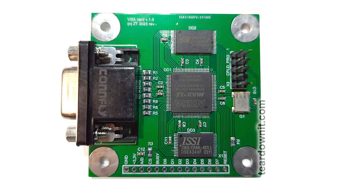 These updates improve overall efficiency by reducing memory access times and using more convenient and modern components, which can also improve product availability and reliability in the future. The updated diagram is shown below: https://assets-global.website-files.com/6438c93ff266bb9903cab3bc/65e96c86ba8d3aa72d43b38e_2003.jpg The timing diagram for new chips has become much more straightforward: https://assets-global.website-files.com/6438c93ff266bb9903cab3bc/65e96c8bd0901fbe1a7f9893_2004.jpg After the final selection of the main components, a printed circuit board, which had specific requirements, was created. The board had to be adapted for manual assembly. Due to this, components were placed on one side of the board, and the number of pinout components was minimized, leaving only external connectors. https://assets-global.website-files.com/6438c93ff266bb9903cab3bc/65e96c95f0ccf2817db63cbf_2005.jpg 50 copies of printed circuit boards were ordered. This introduces the risk of the first boards' errors and inaccuracies, leading to scrapping all fifty and re-ordering the whole batch. Also, along with the boards, a stencil for applying solder paste was ordered. This will simplify the assembly process. While waiting for the boards to be manufactured and delivered, it was time to think about flashing and testing the finished boards. Flashing CPLD was less difficult and could be done using a separate connector and USB programmer. However, programming the character ROM seemed more questionable. On a development board, to reprogram the firmware, the chip had to be carefully removed from the breadboard panel, inserted into the programmer, erased, flashed, removed, and returned to the breadboard panel. These operations turned out to be quite labor-intensive. Therefore, to program the character ROM, it was decided to use the tools of the CPLD itself through a custom parallel interface. There were two possible implementation options: 1. ROM programming with special firmware installed in the CPLD, intended exclusively for ROM programming. 2. Implementation of ROM programming functionality into the working CPLD firmware. The second option was more complex and required additional CPLD resources that would only be used once or twice in the device's lifetime. Fortunately, there were enough CPLD resources available to implement the second option. https://assets-global.website-files.com/6438c93ff266bb9903cab3bc/65e96ca85428c3df3ee6f726_2006.jpg The finished prototype was tested through the same parallel user interface, displaying the test picture on the screen. To do this, I utilized an old laptop with an LPT port, which provided enough I/O lines to transmit all the necessary signals to the device.  The testing device (diagram above) was assembled on a breadboard using the surface-mounting method. The resistors were installed in the housing of the DSUB25 connector, and the tested or programmed board was connected with long and flexible pins. 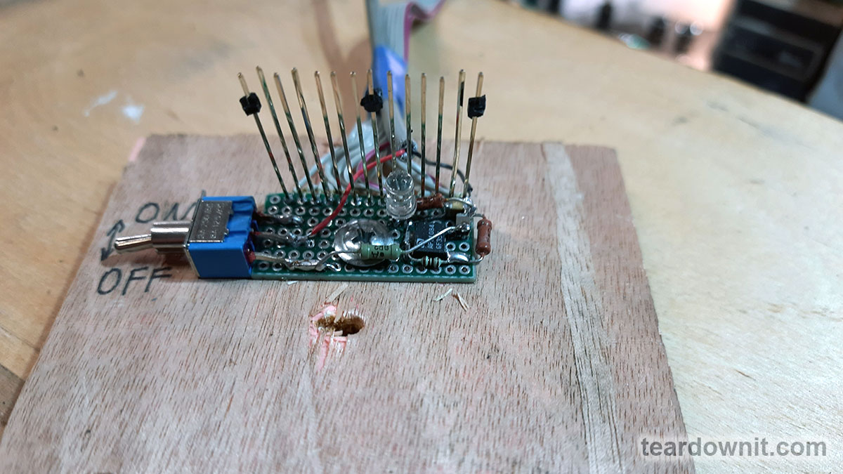 When bending, the contacts create tension in the board hole, ensuring reliable contact. 2 kOhm resistors, together with pull-up resistors of the LPT interface (approximately 1 kOhm), form a voltage divider. This divider converts the 5V logic levels of the LPT port to 3.3V ones. The board is powered through a simple linear stabilizer, getting a voltage of 5 V from the laptop’s USB connector. Resistor R4 with a resistance of 10 ohms is used for current protection. Suppose a short circuit or other problems are on the board under test. In that case, its voltage will decrease, preventing the USB port from overloading. An LED controls a voltage drop of less than 2 V; it will not light up when the power is turned on. 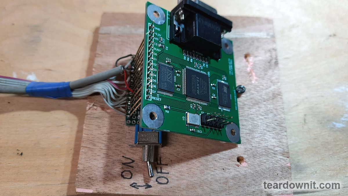 The command-line script for flashing the firmware and testing is written in C. For hardware access to the LPT port, the well-known DLPORTIO drivers are used. It should be noted that these drivers only work fine on Windows XP. 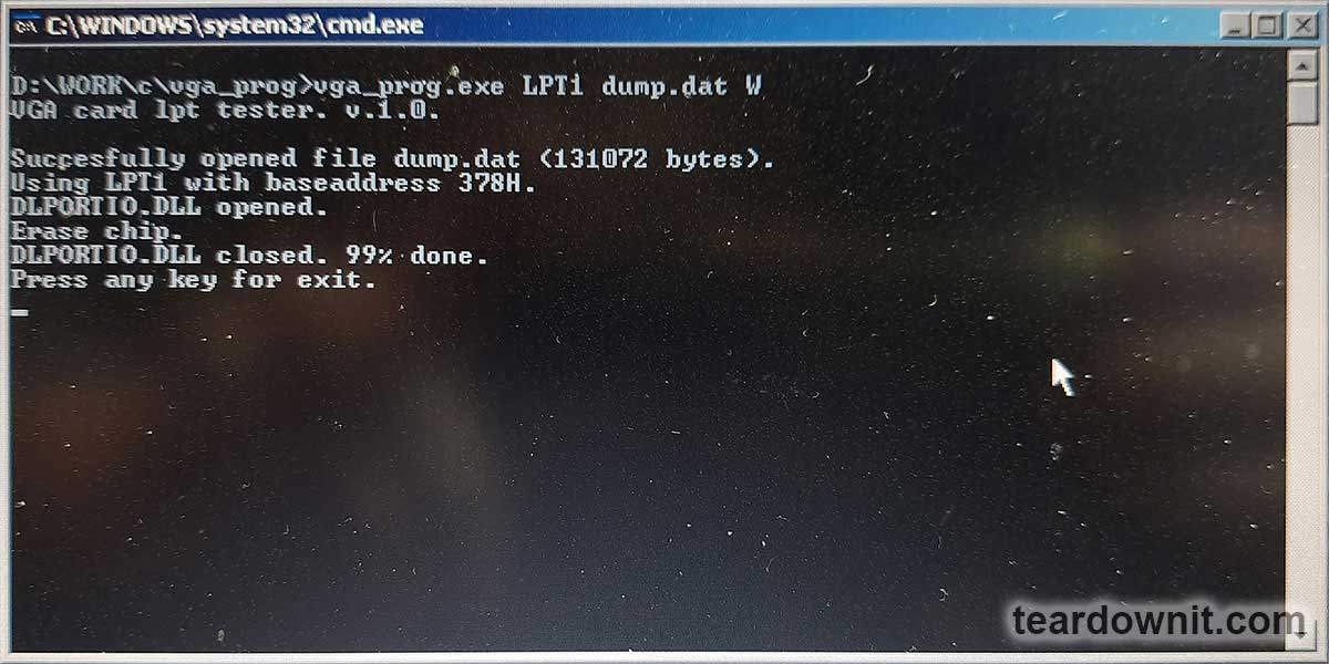 Font files are required to create a dump that will be written to the character generator's ROM. *. FNT files from the MSDOS system or programs of that time are suitable for this. These files contain bit masks of ASCII table characters. For example, in an 8x16 font, each character is described by 16 consecutive bytes.  Modern *. FNT files (as introduced into Windows systems) have a slightly different format. To extract bit masks from them and convert them to the desired format, the script fnt2bin.exe was created. This program takes as input a *. FNT font file with a height of 16 pixels. To convert any other font to the *. FNT format, you can use any free font converter. The result of running the fnt2bin.exe program will be a file of exactly 4096 bytes containing bit masks of the converted font characters. Thus, a dump of the character generator ROM firmware was created, including 32 different fonts. To flash this dump into the ROM using CPLD tools, one of the free bits of the control register was allocated. This bit can only be activated when a RESET signal is present. Upon exiting reset mode, this bit is automatically reset, returning the CPLD to regular operation. After setting this bit, the address setting logic changes, and this address register connects itself to the ROM address bus (not RAM). A 17-bit address is formed in three parts: 6, 6, and 5 bits. The two most significant bits of the address byte determine the "chunk" of the address being written: 00: bits 0 to 5, 01: 6 to 11, 10: bits 12 to 16. Then, one needs to switch to data transfer mode and transfer the data byte written to the ROM chip at the leading edge of the HOST_CS signal. Thus, one packet of address and data to the ROM chip consists of four parts, as shown in the table below. https://assets-global.website-files.com/6438c93ff266bb9903cab3bc/65e96d4e7a2f69433448b634_im2.jpg These messages then form sequences to initiate the byte's flashing. According to the datasheet, there is no "flash completion" flag; it is just waiting for a pause that clearly exceeds the time required for the firmware to flash. https://assets-global.website-files.com/6438c93ff266bb9903cab3bc/65e96d67a872e0b8c7100956_2011.jpg The process is slow, but there is no point in rushing when flashing ROM since writing to the ROM itself takes a lot of time. Additionally, writing to the ROM is typically done only once per device. During software development, the ordered boards, components, and chips arrived. A homemade device was created for applying solder paste. It has a sturdy laminated wood base with stops from PCB scraps to hold the board in place. https://assets-global.website-files.com/6438c93ff266bb9903cab3bc/65e96d6f9cd906453c33856d_2012.jpg The stops were attached with thin, double-sided tape. A sheet of paper placed under the PCB being processed compensated for the height of the tape. This way, the board became perfectly aligned with the stops. A stencil is placed atop the stops, and solder paste is applied. https://assets-global.website-files.com/6438c93ff266bb9903cab3bc/65e96d7546c02e64e8448d90_2013.jpg The components are then placed by hand on the applied solder paste. https://assets-global.website-files.com/6438c93ff266bb9903cab3bc/65e96d7c48eb7b0d0da192a6_2014.jpg Positioning the components precisely is unnecessary since they will drift to their respective places due to surface tension during reflow and become nicely aligned. Although solder paste will stick components to the board, care must be taken not to accidentally dislodge already installed components. Solder reflow is performed using another homemade device. 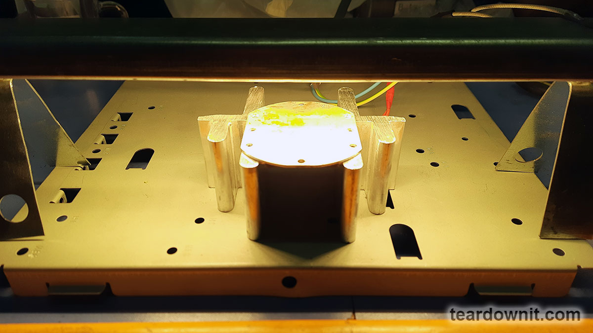 It includes an aluminum heater based on a 300 W thermistor from AliExpress and an IR lamp from the grill of a faulty 600 W microwave oven. Melting occurs very quickly, literally within a few seconds. https://assets-global.website-files.com/6438c93ff266bb9903cab3bc/65e971645428c3df3ee9542c_soldering.gif During reflow, it is essential to keep a close eye on the components and, if necessary, use tweezers to help them move into place, especially if they are not attracted to their pads. If a solder bridge forms on two pins of a chip with a fine pitch, it must be removed using copper braiding. After soldering the surface-mount elements, installing the output elements, such as two connectors, is time. After soldering, a visual inspection is performed, and the remaining flux should be washed off. https://assets-global.website-files.com/6438c93ff266bb9903cab3bc/65e971763566241e63635013_2016.jpg After these steps, the board is installed into the fixture for programming and testing. The test picture is shown in the photo below. https://assets-global.website-files.com/6438c93ff266bb9903cab3bc/65e97181002260b40cbcdfdc_2017.jpg https://assets-global.website-files.com/6438c93ff266bb9903cab3bc/65e97215787e85c46631df92_end.gif After removing the pin shorts and cleaning, it became evident that only 7 out of 20 boards worked. The rest required a more careful inspection for shorts and problematic soldering connections. As a result, 19 boards started working successfully. Still, one board had to be disassembled and reassembled on a new circuit board, and only then was it operational. https://assets-global.website-files.com/6438c93ff266bb9903cab3bc/65e971d2d0901fbe1a8244e1_2018.jpg While working on the board, another idea arose: to use all the device's RAM for 128 characters in 32 lines. This mode would look better on widescreen monitors. This is what the test picture looks like on a widescreen monitor—too much horizontal stretch. https://assets-global.website-files.com/6438c93ff266bb9903cab3bc/65e971dc7a2f6943344b4c92_2019.jpg A temporary firmware was written for CPLD for testing, implementing a non-standard 1024×576 mode. This mode is not on the list of standard supported resolutions. The horizontal parameters were taken from the 1024×768 43 Hz mode and the vertical parameters from the 768×576 60 Hz mode. At a pixel frequency of 50 MHz, the horizontal frequency was 39.55696 kHz, and the refresh rate was 66.25957 Hz. Both of these values are within the acceptable range; for example, the Acer V196HQL monitor, and this monitor displayed the image. The photo below compares an area of 80×30 characters and an area of 128×32. The number of characters is 1.7 times greater. https://assets-global.website-files.com/6438c93ff266bb9903cab3bc/65e971e5ce7c7d70adc92580_2020.jpg However, in this mode, 32 lines of characters use just 512 vertical pixels out of 576. Consequently, 2 lines at the top and 2 lines at the bottom of the image remain empty, and the characters themselves become small and less clear due to the discrepancy between the output and the monitor's native resolution. https://assets-global.website-files.com/6438c93ff266bb9903cab3bc/65e971ec024bd0b87706499b_2021.jpg Since this mode is non-standard, you cannot be sure it will work on all monitors. However, with a high probability, it can be assumed that there will be no issues if the operating frequencies fall within the permissible range. The timing diagram for this version is: 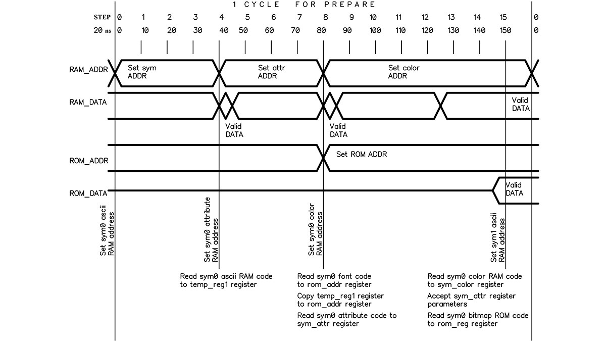 |
| json metadata | {"tags":["videocard"],"image":["https://assets-global.website-files.com/6438c93ff266bb9903cab3bc/65e96c63cafd905222b95c64_2001.jpg","https://cdn.steemitimages.com/DQmRT8AJHhE2Dp6TQR74uRB87QWJdob3gHWUbFiUiQ3U917/image.png","https://assets-global.website-files.com/6438c93ff266bb9903cab3bc/65e96c86ba8d3aa72d43b38e_2003.jpg","https://assets-global.website-files.com/6438c93ff266bb9903cab3bc/65e96c8bd0901fbe1a7f9893_2004.jpg","https://assets-global.website-files.com/6438c93ff266bb9903cab3bc/65e96c95f0ccf2817db63cbf_2005.jpg","https://assets-global.website-files.com/6438c93ff266bb9903cab3bc/65e96ca85428c3df3ee6f726_2006.jpg","https://cdn.steemitimages.com/DQmakKsPQuZD1cCJPc34bWkqp96qWihdRSysAZJzEHspWrQ/image.png","https://cdn.steemitimages.com/DQmd2HUAay34ijrPzFqYk2CVUr2YLnW2tdaV956q6L2nBae/image.png","https://cdn.steemitimages.com/DQmdd1AhyeqamBQNqcEEj8Awd7mbwYWeJHdEmH1V8gJzQQB/image.png","https://cdn.steemitimages.com/DQmQggxFowydzWotkcYaDbh8fuqJxpDbJtdsxjoFbxV7qtP/image.png","https://cdn.steemitimages.com/DQmb3xmMxrChbMYCtHjVtjxiz7SBGtbEv6cDxjVZf4W1hxX/image.png","https://assets-global.website-files.com/6438c93ff266bb9903cab3bc/65e96d4e7a2f69433448b634_im2.jpg","https://assets-global.website-files.com/6438c93ff266bb9903cab3bc/65e96d67a872e0b8c7100956_2011.jpg","https://assets-global.website-files.com/6438c93ff266bb9903cab3bc/65e96d6f9cd906453c33856d_2012.jpg","https://assets-global.website-files.com/6438c93ff266bb9903cab3bc/65e96d7546c02e64e8448d90_2013.jpg","https://assets-global.website-files.com/6438c93ff266bb9903cab3bc/65e96d7c48eb7b0d0da192a6_2014.jpg","https://cdn.steemitimages.com/DQmR4qB74hh51JCnFzre1m4MZzbESCu3KeYVfDNDNzj5EBU/image.png","https://assets-global.website-files.com/6438c93ff266bb9903cab3bc/65e971645428c3df3ee9542c_soldering.gif","https://assets-global.website-files.com/6438c93ff266bb9903cab3bc/65e971763566241e63635013_2016.jpg","https://assets-global.website-files.com/6438c93ff266bb9903cab3bc/65e97181002260b40cbcdfdc_2017.jpg","https://assets-global.website-files.com/6438c93ff266bb9903cab3bc/65e97215787e85c46631df92_end.gif","https://assets-global.website-files.com/6438c93ff266bb9903cab3bc/65e971d2d0901fbe1a8244e1_2018.jpg","https://assets-global.website-files.com/6438c93ff266bb9903cab3bc/65e971dc7a2f6943344b4c92_2019.jpg","https://assets-global.website-files.com/6438c93ff266bb9903cab3bc/65e971e5ce7c7d70adc92580_2020.jpg","https://assets-global.website-files.com/6438c93ff266bb9903cab3bc/65e971ec024bd0b87706499b_2021.jpg","https://cdn.steemitimages.com/DQmXTUoq6dmvSjqkvoovJCtN4yD6EQ7ivstcxvSdPfhLzsn/image.png"],"app":"steemit/0.2","format":"markdown"} |
| parent author | |
| parent permlink | videocard |
| permlink | vga-videocard-for-microcontrollers-part-2 |
| title | VGA videocard for microcontrollers. Part 2 |
| Transaction Info | Block #83361033/Trx a9692c64b775af0b5978a53ee22735a652cee5b9 |
View Raw JSON Data
{
"block": 83361033,
"op": [
"comment",
{
"author": "teardownit",
"body": "https://assets-global.website-files.com/6438c93ff266bb9903cab3bc/65e96c63cafd905222b95c64_2001.jpg\n\nFirst of all, you should pay attention to the ROM used. The flash-ROM chip from an old computer motherboard has a finicky parallel interface where the address is written in two runs. This complicates the operating logic and increases access time. Additionally, the PLCC housing it comes in can be expensive and challenging to install manually. In this regard, it was decided to replace it with a more modern 39-series microchip from SST. These chips, such as the SST39LF and SST39VF, have faster access times (55 ns and 70 ns, respectively) compared to 270 ns for the 49 series chip. This allows one to reduce data preparation time to one cycle. The SST39VF010-70-4C-WHE chip has been ordered.\n\nIt is also necessary to replace the RAM. To save money, I picked one that operates precisely at 3.3 V and has TSOP housing. The IS62LV256AL-45TLI chip was ordered.\n\nThe CPLD chip remains unchanged.\n\n\n\n\nThese updates improve overall efficiency by reducing memory access times and using more convenient and modern components, which can also improve product availability and reliability in the future.\n\nThe updated diagram is shown below:\n\nhttps://assets-global.website-files.com/6438c93ff266bb9903cab3bc/65e96c86ba8d3aa72d43b38e_2003.jpg\nThe timing diagram for new chips has become much more straightforward:\n\nhttps://assets-global.website-files.com/6438c93ff266bb9903cab3bc/65e96c8bd0901fbe1a7f9893_2004.jpg\n\nAfter the final selection of the main components, a printed circuit board, which had specific requirements, was created. The board had to be adapted for manual assembly. Due to this, components were placed on one side of the board, and the number of pinout components was minimized, leaving only external connectors.\n\nhttps://assets-global.website-files.com/6438c93ff266bb9903cab3bc/65e96c95f0ccf2817db63cbf_2005.jpg\n50 copies of printed circuit boards were ordered. This introduces the risk of the first boards' errors and inaccuracies, leading to scrapping all fifty and re-ordering the whole batch. Also, along with the boards, a stencil for applying solder paste was ordered. This will simplify the assembly process.\n\nWhile waiting for the boards to be manufactured and delivered, it was time to think about flashing and testing the finished boards. Flashing CPLD was less difficult and could be done using a separate connector and USB programmer. However, programming the character ROM seemed more questionable. On a development board, to reprogram the firmware, the chip had to be carefully removed from the breadboard panel, inserted into the programmer, erased, flashed, removed, and returned to the breadboard panel. These operations turned out to be quite labor-intensive.\nTherefore, to program the character ROM, it was decided to use the tools of the CPLD itself through a custom parallel interface. There were two possible implementation options:\n\n1. ROM programming with special firmware installed in the CPLD, intended exclusively for ROM programming.\n2. Implementation of ROM programming functionality into the working CPLD firmware.\n\nThe second option was more complex and required additional CPLD resources that would only be used once or twice in the device's lifetime. Fortunately, there were enough CPLD resources available to implement the second option.\nhttps://assets-global.website-files.com/6438c93ff266bb9903cab3bc/65e96ca85428c3df3ee6f726_2006.jpg\n\nThe finished prototype was tested through the same parallel user interface, displaying the test picture on the screen. To do this, I utilized an old laptop with an LPT port, which provided enough I/O lines to transmit all the necessary signals to the device.\n\n\n\nThe testing device (diagram above) was assembled on a breadboard using the surface-mounting method. The resistors were installed in the housing of the DSUB25 connector, and the tested or programmed board was connected with long and flexible pins.\n\n\n\nWhen bending, the contacts create tension in the board hole, ensuring reliable contact. 2 kOhm resistors, together with pull-up resistors of the LPT interface (approximately 1 kOhm), form a voltage divider. This divider converts the 5V logic levels of the LPT port to 3.3V ones.\n\nThe board is powered through a simple linear stabilizer, getting a voltage of 5 V from the laptop’s USB connector. Resistor R4 with a resistance of 10 ohms is used for current protection. Suppose a short circuit or other problems are on the board under test. In that case, its voltage will decrease, preventing the USB port from overloading. An LED controls a voltage drop of less than 2 V; it will not light up when the power is turned on.\n\n\n\nThe command-line script for flashing the firmware and testing is written in C. For hardware access to the LPT port, the well-known DLPORTIO drivers are used. It should be noted that these drivers only work fine on Windows XP.\n\n\n\nFont files are required to create a dump that will be written to the character generator's ROM. *. FNT files from the MSDOS system or programs of that time are suitable for this. These files contain bit masks of ASCII table characters. For example, in an 8x16 font, each character is described by 16 consecutive bytes.\n\n\n\nModern *. FNT files (as introduced into Windows systems) have a slightly different format. To extract bit masks from them and convert them to the desired format, the script fnt2bin.exe was created. This program takes as input a *. FNT font file with a height of 16 pixels. To convert any other font to the *. FNT format, you can use any free font converter. The result of running the fnt2bin.exe program will be a file of exactly 4096 bytes containing bit masks of the converted font characters. Thus, a dump of the character generator ROM firmware was created, including 32 different fonts.\n\nTo flash this dump into the ROM using CPLD tools, one of the free bits of the control register was allocated. This bit can only be activated when a RESET signal is present. Upon exiting reset mode, this bit is automatically reset, returning the CPLD to regular operation. After setting this bit, the address setting logic changes, and this address register connects itself to the ROM address bus (not RAM). A 17-bit address is formed in three parts: 6, 6, and 5 bits. The two most significant bits of the address byte determine the \"chunk\" of the address being written: 00: bits 0 to 5, 01: 6 to 11, 10: bits 12 to 16. Then, one needs to switch to data transfer mode and transfer the data byte written to the ROM chip at the leading edge of the HOST_CS signal. Thus, one packet of address and data to the ROM chip consists of four parts, as shown in the table below.\n\nhttps://assets-global.website-files.com/6438c93ff266bb9903cab3bc/65e96d4e7a2f69433448b634_im2.jpg\n\nThese messages then form sequences to initiate the byte's flashing. According to the datasheet, there is no \"flash completion\" flag; it is just waiting for a pause that clearly exceeds the time required for the firmware to flash.\n\nhttps://assets-global.website-files.com/6438c93ff266bb9903cab3bc/65e96d67a872e0b8c7100956_2011.jpg\n\nThe process is slow, but there is no point in rushing when flashing ROM since writing to the ROM itself takes a lot of time. Additionally, writing to the ROM is typically done only once per device.\n\nDuring software development, the ordered boards, components, and chips arrived. A homemade device was created for applying solder paste. It has a sturdy laminated wood base with stops from PCB scraps to hold the board in place.\n\nhttps://assets-global.website-files.com/6438c93ff266bb9903cab3bc/65e96d6f9cd906453c33856d_2012.jpg\n\nThe stops were attached with thin, double-sided tape. A sheet of paper placed under the PCB being processed compensated for the height of the tape. This way, the board became perfectly aligned with the stops.\n\nA stencil is placed atop the stops, and solder paste is applied.\n\nhttps://assets-global.website-files.com/6438c93ff266bb9903cab3bc/65e96d7546c02e64e8448d90_2013.jpg\n\nThe components are then placed by hand on the applied solder paste.\n\nhttps://assets-global.website-files.com/6438c93ff266bb9903cab3bc/65e96d7c48eb7b0d0da192a6_2014.jpg\n\nPositioning the components precisely is unnecessary since they will drift to their respective places due to surface tension during reflow and become nicely aligned. Although solder paste will stick components to the board, care must be taken not to accidentally dislodge already installed components.\n\nSolder reflow is performed using another homemade device.\n\n\n\nIt includes an aluminum heater based on a 300 W thermistor from AliExpress and an IR lamp from the grill of a faulty 600 W microwave oven. Melting occurs very quickly, literally within a few seconds.\n\nhttps://assets-global.website-files.com/6438c93ff266bb9903cab3bc/65e971645428c3df3ee9542c_soldering.gif\n\nDuring reflow, it is essential to keep a close eye on the components and, if necessary, use tweezers to help them move into place, especially if they are not attracted to their pads. If a solder bridge forms on two pins of a chip with a fine pitch, it must be removed using copper braiding.\n\nAfter soldering the surface-mount elements, installing the output elements, such as two connectors, is time. After soldering, a visual inspection is performed, and the remaining flux should be washed off.\n\nhttps://assets-global.website-files.com/6438c93ff266bb9903cab3bc/65e971763566241e63635013_2016.jpg\n\nAfter these steps, the board is installed into the fixture for programming and testing. The test picture is shown in the photo below.\n\nhttps://assets-global.website-files.com/6438c93ff266bb9903cab3bc/65e97181002260b40cbcdfdc_2017.jpg\n\nhttps://assets-global.website-files.com/6438c93ff266bb9903cab3bc/65e97215787e85c46631df92_end.gif\n\nAfter removing the pin shorts and cleaning, it became evident that only 7 out of 20 boards worked. The rest required a more careful inspection for shorts and problematic soldering connections. As a result, 19 boards started working successfully. Still, one board had to be disassembled and reassembled on a new circuit board, and only then was it operational.\n\nhttps://assets-global.website-files.com/6438c93ff266bb9903cab3bc/65e971d2d0901fbe1a8244e1_2018.jpg\n\nWhile working on the board, another idea arose: to use all the device's RAM for 128 characters in 32 lines. This mode would look better on widescreen monitors. This is what the test picture looks like on a widescreen monitor—too much horizontal stretch.\n\nhttps://assets-global.website-files.com/6438c93ff266bb9903cab3bc/65e971dc7a2f6943344b4c92_2019.jpg\n\nA temporary firmware was written for CPLD for testing, implementing a non-standard 1024×576 mode. This mode is not on the list of standard supported resolutions.\n\nThe horizontal parameters were taken from the 1024×768 43 Hz mode and the vertical parameters from the 768×576 60 Hz mode. At a pixel frequency of 50 MHz, the horizontal frequency was 39.55696 kHz, and the refresh rate was 66.25957 Hz. Both of these values are within the acceptable range; for example, the Acer V196HQL monitor, and this monitor displayed the image.\nThe photo below compares an area of 80×30 characters and an area of 128×32. The number of characters is 1.7 times greater.\n\nhttps://assets-global.website-files.com/6438c93ff266bb9903cab3bc/65e971e5ce7c7d70adc92580_2020.jpg\n\nHowever, in this mode, 32 lines of characters use just 512 vertical pixels out of 576. Consequently, 2 lines at the top and 2 lines at the bottom of the image remain empty, and the characters themselves become small and less clear due to the discrepancy between the output and the monitor's native resolution.\n\nhttps://assets-global.website-files.com/6438c93ff266bb9903cab3bc/65e971ec024bd0b87706499b_2021.jpg\n\nSince this mode is non-standard, you cannot be sure it will work on all monitors. However, with a high probability, it can be assumed that there will be no issues if the operating frequencies fall within the permissible range.\n\nThe timing diagram for this version is:\n\n",
"json_metadata": "{\"tags\":[\"videocard\"],\"image\":[\"https://assets-global.website-files.com/6438c93ff266bb9903cab3bc/65e96c63cafd905222b95c64_2001.jpg\",\"https://cdn.steemitimages.com/DQmRT8AJHhE2Dp6TQR74uRB87QWJdob3gHWUbFiUiQ3U917/image.png\",\"https://assets-global.website-files.com/6438c93ff266bb9903cab3bc/65e96c86ba8d3aa72d43b38e_2003.jpg\",\"https://assets-global.website-files.com/6438c93ff266bb9903cab3bc/65e96c8bd0901fbe1a7f9893_2004.jpg\",\"https://assets-global.website-files.com/6438c93ff266bb9903cab3bc/65e96c95f0ccf2817db63cbf_2005.jpg\",\"https://assets-global.website-files.com/6438c93ff266bb9903cab3bc/65e96ca85428c3df3ee6f726_2006.jpg\",\"https://cdn.steemitimages.com/DQmakKsPQuZD1cCJPc34bWkqp96qWihdRSysAZJzEHspWrQ/image.png\",\"https://cdn.steemitimages.com/DQmd2HUAay34ijrPzFqYk2CVUr2YLnW2tdaV956q6L2nBae/image.png\",\"https://cdn.steemitimages.com/DQmdd1AhyeqamBQNqcEEj8Awd7mbwYWeJHdEmH1V8gJzQQB/image.png\",\"https://cdn.steemitimages.com/DQmQggxFowydzWotkcYaDbh8fuqJxpDbJtdsxjoFbxV7qtP/image.png\",\"https://cdn.steemitimages.com/DQmb3xmMxrChbMYCtHjVtjxiz7SBGtbEv6cDxjVZf4W1hxX/image.png\",\"https://assets-global.website-files.com/6438c93ff266bb9903cab3bc/65e96d4e7a2f69433448b634_im2.jpg\",\"https://assets-global.website-files.com/6438c93ff266bb9903cab3bc/65e96d67a872e0b8c7100956_2011.jpg\",\"https://assets-global.website-files.com/6438c93ff266bb9903cab3bc/65e96d6f9cd906453c33856d_2012.jpg\",\"https://assets-global.website-files.com/6438c93ff266bb9903cab3bc/65e96d7546c02e64e8448d90_2013.jpg\",\"https://assets-global.website-files.com/6438c93ff266bb9903cab3bc/65e96d7c48eb7b0d0da192a6_2014.jpg\",\"https://cdn.steemitimages.com/DQmR4qB74hh51JCnFzre1m4MZzbESCu3KeYVfDNDNzj5EBU/image.png\",\"https://assets-global.website-files.com/6438c93ff266bb9903cab3bc/65e971645428c3df3ee9542c_soldering.gif\",\"https://assets-global.website-files.com/6438c93ff266bb9903cab3bc/65e971763566241e63635013_2016.jpg\",\"https://assets-global.website-files.com/6438c93ff266bb9903cab3bc/65e97181002260b40cbcdfdc_2017.jpg\",\"https://assets-global.website-files.com/6438c93ff266bb9903cab3bc/65e97215787e85c46631df92_end.gif\",\"https://assets-global.website-files.com/6438c93ff266bb9903cab3bc/65e971d2d0901fbe1a8244e1_2018.jpg\",\"https://assets-global.website-files.com/6438c93ff266bb9903cab3bc/65e971dc7a2f6943344b4c92_2019.jpg\",\"https://assets-global.website-files.com/6438c93ff266bb9903cab3bc/65e971e5ce7c7d70adc92580_2020.jpg\",\"https://assets-global.website-files.com/6438c93ff266bb9903cab3bc/65e971ec024bd0b87706499b_2021.jpg\",\"https://cdn.steemitimages.com/DQmXTUoq6dmvSjqkvoovJCtN4yD6EQ7ivstcxvSdPfhLzsn/image.png\"],\"app\":\"steemit/0.2\",\"format\":\"markdown\"}",
"parent_author": "",
"parent_permlink": "videocard",
"permlink": "vga-videocard-for-microcontrollers-part-2",
"title": "VGA videocard for microcontrollers. Part 2"
}
],
"op_in_trx": 0,
"timestamp": "2024-03-15T08:08:30",
"trx_id": "a9692c64b775af0b5978a53ee22735a652cee5b9",
"trx_in_block": 0,
"virtual_op": 0
}bluesnipersent 0.010 STEEM to @teardownit- "Hello. Good to see you on Steem. To maximize your rewards, publish your post also on Hive ( hive.blog ) and Blurt ( blurt.blog ) blockchains. Use upvu, jsup or ctime and get instant upvotes"2024/03/13 08:17:21
bluesnipersent 0.010 STEEM to @teardownit- "Hello. Good to see you on Steem. To maximize your rewards, publish your post also on Hive ( hive.blog ) and Blurt ( blurt.blog ) blockchains. Use upvu, jsup or ctime and get instant upvotes"
2024/03/13 08:17:21
| amount | 0.010 STEEM |
| from | bluesniper |
| memo | Hello. Good to see you on Steem. To maximize your rewards, publish your post also on Hive ( hive.blog ) and Blurt ( blurt.blog ) blockchains. Use upvu, jsup or ctime and get instant upvotes |
| to | teardownit |
| Transaction Info | Block #83304566/Trx f95e519feea0e2ec8cd924631186e64dec8e0e2a |
View Raw JSON Data
{
  "block": 83304566,
  "op": [
    "transfer",
    {
      "amount": "0.010 STEEM",
      "from": "bluesniper",
      "memo": "Hello. Good to see you on Steem. To maximize your rewards, publish your post also on Hive ( hive.blog ) and Blurt ( blurt.blog ) blockchains. Use upvu, jsup or ctime and get instant upvotes",
      "to": "teardownit"
    }
  ],
  "op_in_trx": 0,
  "timestamp": "2024-03-13T08:17:21",
  "trx_id": "f95e519feea0e2ec8cd924631186e64dec8e0e2a",
  "trx_in_block": 0,
  "virtual_op": 0
}bluesniperupvoted (100.00%) @teardownit / vga-videocard-for-microcontrollers-part-12024/03/13 08:16:57
bluesniperupvoted (100.00%) @teardownit / vga-videocard-for-microcontrollers-part-1
2024/03/13 08:16:57
| author | teardownit |
| permlink | vga-videocard-for-microcontrollers-part-1 |
| voter | bluesniper |
| weight | 10000 (100.00%) |
| Transaction Info | Block #83304558/Trx 6ebf5a87c3b3f9c8b263e002ed0d0aaed3f6f823 |
View Raw JSON Data
{
  "block": 83304558,
  "op": [
    "vote",
    {
      "author": "teardownit",
      "permlink": "vga-videocard-for-microcontrollers-part-1",
      "voter": "bluesniper",
      "weight": 10000
    }
  ],
  "op_in_trx": 0,
  "timestamp": "2024-03-13T08:16:57",
  "trx_id": "6ebf5a87c3b3f9c8b263e002ed0d0aaed3f6f823",
  "trx_in_block": 1,
  "virtual_op": 0
}teardownitpublished a new post: vga-videocard-for-microcontrollers-part-12024/03/13 08:11:27
teardownitpublished a new post: vga-videocard-for-microcontrollers-part-1
2024/03/13 08:11:27
| author | teardownit |
| body | https://assets-global.website-files.com/6438c93ff266bb9903cab3bc/65e59b391c8b1c9c28225a4a_1001.jpg Sometimes, when making your own devices on microcontrollers, there is a need to display huge amounts of information on a display and to use a bigger screen for ease of perception. Unfortunately, there are no ready-made and budget-friendly solutions for this task on the market. LCD displays with the ability to connect to a microcontroller are usually tiny and pricy. But at the same time, there is a wide selection of legacy LCD monitors with a VGA interface. Models with a diagonal of 15 to 19 inches can be purchased in perfect working condition for a very low price, or one can even get one for free. This especially applies to monitors with a 4:3 aspect ratio. In addition, such models are usually quite reliable. Most older monitors only have a VGA connector for connecting to a computer. Sometimes there is an additional DVI port (on more expensive models). The HDMI connector is more common on modern devices. Thus, with a probability close to 100%, we'll get just a VGA on an older monitor. In order to display an image on such a monitor, it is enough to work with only five signals: analog R (red), G (green), and B (blue), responsible for the brightness of each color component, as well as digital HS (horizontal sync) and VS (vertical sync), providing synchronization. Analogue signal levels should range from 0 to 0.7 V, where 0 V corresponds to no light at all and 0.7 V to maximum brightness. Digital signals HS and VS are short pulses with a TTL level of negative polarity. The timings of these signals can be found, for example, here: http://tinyvga.com/vga-timing/640x480@60Hz. Typically, special controllers, or FPGAs, are used to generate video signals, and many FPGA development boards are already equipped with a VGA connector. However, FPGAs are often expensive and require many additional components. I was looking for a simpler and cheaper solution. As a result, the decision was made to use CPLD. CPLDs have fewer available logic gates (LEs) than FPGAs but are less expensive. For example, the MAX II Altera EPM240 development board is sold on Aliexpress: https://www.aliexpress.us/item/3256804686276488.html for only $8.12 (excluding shipping), and the kit even includes a programmer. The chips themselves can be purchased for $1.6–2.1 (for nice knockoffs). https://assets-global.website-files.com/6438c93ff266bb9903cab3bc/65e59bec6d4e1824cd947b1b_1002.jpg Plain text mode was chosen for implementation because it is easier for a slow microcontroller but at the same time quite informative. Some graphics elements can be implemented using pseudo-graphics symbols, as was often done in the days of DOS. The introduction of a graphics mode would require transferring a large amount of data from the microcontroller and additional efforts to create it, which is not always possible, especially for weak cores. CPLD has a built-in Flash ROM (User Flash Memory block, UFM), which can be used as a character ROM. However, its capacity is very limited—only 8 kbit, or 1 KB. This amount of storage is only sufficient for characters with a resolution of 5×7 pixels, and only if we discard non-displayable, insignificant, and visually identical characters from the ASCII table. In addition, the use of UFM will require the use of logic gates (LE), of which there are already a few. Despite the attractiveness of this option, I had to abandon it and use an external ROM chip, which can be salvaged from an old motherboard. Choosing a microchip with a supply voltage of 3.3 V will eliminate problems with matching voltage levels for the CPLD. The capacity of such ROMs is quite large: 2, 4, or 8 Mbit, or at least 256 to 1024 KB, which allows one to store a large number of different fonts with a decent resolution of 8x16 pixels. https://assets-global.website-files.com/6438c93ff266bb9903cab3bc/65e59bf7f6aa7cdb65960c59_1003.jpg To store the screen image, you will also need a RAM chip. Let's estimate the approximate size required for this. If we plan on using an 8×16 pixel font on a screen with a resolution of 640×480 pixels, we will end up with 80 characters per line and 30 lines on the screen. Thus, saving the screen image will require 80 × 30 = 2400 bytes. This number is somewhat inconvenient because it is just slightly larger than the nearest power of two, 2048. The memory use in this case is inefficient—only 58%, since the next power of two is 4096. By the way, this is exactly why text mode with 80×25 symbols became popular since there are 5 fewer lines on the screen. In this case, only 2000 bytes of memory are needed, which easily fits into 2 KB. However, modern memory chips have significant storage sizes, and saving memory is not so critical nowadays. Moreover, one can deliberately choose to waste memory in order to simplify the decryption logic and save CPLD logic elements. Then you will need at least 4096 bytes (2^12, 12 address bits), which can be divided as follows: 5 address bits are allocated to the row address on the screen (30 of 32 will be used) and 7 bits to the column or position address characters in the string (80 out of 128 will be used). 4096 bytes are required only for storing ASCII symbols. The same amount of memory will be taken by the symbol attribute page. Attributes must include character color (3 bits), background color (3 bits), underline, and blinking. So, a memory of at least 8 KB is required. Of the most affordable options, the best one is static RAM (used as cache memory), also salvaged from old devices or motherboards. It should be noted that this memory can only operate at 5 V. However. If it is a CMOS-type memory, it can take 3.3 V, but this will require timing correction. So, we got the following diagram:. https://assets-global.website-files.com/6438c93ff266bb9903cab3bc/65e59c032f79e7ab7614aa4f_1004.jpg The circuit includes only three microchips and a minimum number of external components. Using the aforementioned Altera EPM240 development board as a base, all you need are ROM chips, RAM chips, and a DSUB header with five resistors. Connecting signals to the CPLD is just an approximation, since almost all of its pins are equivalent (with the exception of Global CLK, one of which requires connecting a signal from a clock generator). When the chip is repeatedly reprogrammed for a new device, almost all of its signals can be reassigned. Currently, the device is assembled on a breadboard and can be left aside. The device communicates with the microcontroller via a parallel 8-bit interface (in the diagram, signals with the HOST prefix), which is logically almost identical to the widely used display interface on the 1602 and similar controllers. The only difference is the addition of a BUSY signal directed from the device to the microcontroller. Its necessity is due to the fact that access to the RAM chip is provided only during the backward sweep period. The rest of the time, the chip is busy (pun intended) executing CPLD logic. The BUSY signal also acts like an interrupt request (IRQ) function. When it's changed, the controller can automatically start writing to the screen buffer. Interface description: DATA[7:0] – eight bits of data, unidirectional port, intended exclusively for writing to the device CS – chip select; 0 for chip is selected, 1 for chip is not selected. On the positive edge of the CS signal, the data is latched for writing. AD – address/data, during a write operation: 0 – data is being transferred; 1 – address is being transferred. BUSY – device busy state; 0 – free; 1 – busy. If the device is busy, the write operation to RAM is ignored. Writing is only possible to the address register. RESET – device reset. 0 – reset; 1 – work. A hard reset can be used to turn off the screen immediately. When this signal is activated, the image output to the monitor stops. Resetting does not affect the contents of the RAM chip. Writing data from the microcontroller to RAM is possible only during the backward sweep of the frame scan, when the RAM chip is not occupied by the CPLD logic. This time interval is 1.440 milliseconds. Despite the significant duration of this interval, when using slow microcontrollers, there may not be enough time to completely rewrite the entire memory space. For example, an AVR microcontroller, when operating at a frequency of 11.0592 MHz, is capable of recording only three full-screen lines with all the attributes. If one does not update the attributes (as is usually the case in real-life applications, attributes are written once when the program starts), then six full rows can be written in this time. Perhaps optimizing the code and rewriting it in assembly language can significantly speed up the process of updating data. Otherwise, it may take from 5 cycles (if updating only the data) to 15 cycles (if updating the attributes) to completely rewrite the screen. At 60 fps, it will take 1/12 to 1/4 of a second. Those who have ever worked on IBM PC/XT or IBM PC/AT computers with processor clock speeds around 4 to 12 MHz may notice the experience of refreshing the screen to be familiar. If you don’t want to wait for the next vertical pulse and want to record all the data at once, you can use the RESET signal. When activated, the internal logic of the CPLD stops and is disconnected from the RAM chip, allowing the microcontroller to directly access the memory. Registers for working with RAM are not affected by the reset signal. In general, the write operations are as follows: you need to wait until the BUSY signal becomes zero, then put the desired data on the data bus, set the data type (address or data) AD, and set the CS signal first to 0, then to 1. When this signal changes from 0 to 1, the data is stored in memory. During a vertical pulse, the RAM chip is directly connected to the microcontroller's HOST signals, so maintaining the timings during writes becomes the responsibility of the microcontroller. However, since static RAM is a fairly fast device and typically has timings significantly smaller than the maximum speed of an average microcontroller driving its I/O lines, this task is not difficult. The RAM chip D43256BGU-70LL is connected to the CPLD's output pins, with the lines having a 'RAM' prefix on the diagram. These signals include an 8-bit bidirectional data bus and a 13-bit address bus. Of the control signals, only the WE signal is used. Since there is only one chip on the RAM bus and both buses (address and data) are completely under its control, the OE and CS signals are not used, equal 0, and connected to GND. The SST49LF002A ROM chip is connected similarly (signals with the 'ROM' prefix), except that the data bus in this case is unidirectional. The OE and WE signals of this IC are also not used and are directly connected to 0 (GND) and 1 (VCC), respectively. Jumpers are connected to the available CPLD pins to select the current font. Since the ROM chip is large enough, it allows one to store several different fonts, including national alphabets, and switch to them by installing jumpers. The DSUB VGA port is connected to the CPLD using only 5 resistors. Resistors in the HS and VS circuits are primarily for protection and can be ditched. Resistors in circuits R, G, and B are selected in such a way that, together with the input resistance of the monitor (75 Ohms), they form a voltage divider that reduces the voltage at the monitor input to 0.7 V. The power leads are shunted with ceramic capacitors, and the clock signal with a frequency of 50 MHz from a crystal is supplied to the GCLK0 pin. These parts were on the breadboard originally. A resistor, a capacitor, and a button are connected to the RESET signal, forming it. However, if the signal is generated by a microcontroller, these components are redundant. After creating the main part of the CPLD operating logic, it became clear that the number of logic elements (LEs) used was slightly over half of the available ones. In this regard, the idea arose to complexify the logic and add more features. First of all, the number of colors can be increased to 16 by adding three additional CPLD pins and three resistors. This won't significantly complicate the scheme, but it will add eight more colors. In this case, the RAM page with attributes will have to be completely devoted to color, and another page with attributes will have to be added, increasing the RAM address bus by 1 bit. In the second page of attributes, you can implement font selection, underlining, character and background flickering, and so on. The new scheme looks similar to the previous one. https://assets-global.website-files.com/6438c93ff266bb9903cab3bc/65e59c50b01293d756c1a42f_1005.jpg As the number of colors increases, the question is: which palette to choose? With only 8 colors, there is no such question; all colors are different combinations of the three primary colors: red, green, and blue (2^3 = 8). When there are more colors, different options are possible. For example, the 16-color EGA palette: https://moddingwiki.shikadi.net/wiki/EGA_Palette:  As can be seen from the presented palette, the 4th bit in the color number stands for brightness. However, the halves of the table are not evenly separated by brightness. The first half is set to 2/3 brightness (byte AAH = 170 = 2/3 × 256). In the second half, another 1/3 of brightness is added (byte 55H = 85 = 1/3 × 256), and the colors in this part are called "bright." Interestingly, color No. 6 (yellow/brown) in this scheme deviates from the expected AAAA00 and is specifically set to AA5500. This was done to replace the unattractive, dirty yellow color with the more appealing brown. This is a known feature of EGA video cards and monitors. Some monitors took this into account, while others did not implement this feature in order to simplify the circuit. Some models added a BROWN ADJ knob so that the user could set the desired shade of that color. That is why the color in the table is indicated as yellow/brown. Nonlinear separation by brightness level automatically leads to two shades of gray showing up: light gray and dark gray, which are widely used. In the 16-color VGA palette: https://lospec.com/palette-list/microsoft-vga, the situation is slightly different: the colors are divided exactly in two halves by brightness (80H = 128 = 1/2 × 256): https://assets-global.website-files.com/6438c93ff266bb9903cab3bc/65e59ca72c6395d0e38158f4_1007.jpg There is also a noticeable outlier in this palette: light gray (С0С0С0), which should be black, duplicating an existing color. Additionally, this color swapped places with the dark gray color (808080). This was done intentionally to ensure compatibility between the VGA and EGA 16-color palettes, making them almost identical. In our case, when the R, G, and B signals are generated in hardware using resistors, it is more convenient to use the EGA palette. So, it is necessary to make a software correction only for one color, No. 6. All other colors are generated automatically. Switching to the VGA palette would require not only a program change but also an additional group of resistors to be added to create the light gray color (C0C0C0). The resistors should be picked so that one group provides a brightness level of 1/3, the second is 2/3, and together they provide full brightness. By simple calculations using Ohm's law, we get the following values: 390 Ohms and 750 Ohms. The signal generation logic for a static image like the one with test color bars is quite simple. However, if it is necessary to generate a dynamic image, the task becomes more complicated. It is necessary to organize a logical interface with RAM and ROM. At the same time, data exchange should occur not just quickly but lightning-fast! Let's first evaluate whether the selected chips can keep up with operating like this. So, the resolution is 640x480. Pixel output frequency is 25 MHz (the standard specifies 25.175 MHz, but rounding to 25 MHz is acceptable since VGA, like many other analog standards, allows a significant spread of parameters). The frame refresh rate is 60 Hz (actually 59.5 Hz), and the line refresh rate is 31.46875 kHz (actually 31.25 kHz). Thus, the output time of one pixel is 40 ns, and the output time of an 8-bit character is 320 ns. During this time, the ASCII code of the character (one byte), the color code (one byte), and the attributes (one byte) should be read from RAM, and then, using the ASCII code as an address, we should read the bit mask of the character from ROM. Only then will the CPLD logic have all the necessary information to begin imaging. According to the technical description (datasheet), for the selected D43256BGU-70LL chip, a full read cycle takes 70 ns. Considering the use of the chip at reduced voltage, the read cycle takes longer—let's say, 100 ns. Thus, in 320 ns, we will have enough time to read three bytes from RAM: ASCII code, color code, and character attributes. Great. The situation with ROM is more complicated: the address is written to it in two steps—in rows and columns—and, according to the manual, the read cycle takes 270 ns. Not the highest speed, but within the required 320 ns, even with time to spare. The problem is that we can't start issuing the ROM address until we know at least the ASCII code, which takes 100 ns. This sums up to 370 ns. What saves us is the fact that each RAM or ROM read cycle individually fits within the allowed interval, and we can simply spend two additional cycles reading data. To add these two loops during data preparation, it is necessary to shift the character display area, creating an additional blanking area 2 characters wide at the beginning of the line and reducing the same area at the end of the line by 2 characters. This is quite simple to do: we simply shift the horizontal blanking pulse by 640 ns (accordingly, the horizontal sync pulse also shifts). From the monitor's point of view, there is no difference. To better understand when and what to write and read, it is handy to create a timing diagram. At the beginning, all the timings were in my head, but creating a paper diagram and giving it another look allowed me to significantly optimize read cycles and even reduce the number of registers used. https://assets-global.website-files.com/6438c93ff266bb9903cab3bc/65e59cc7155593c32699ee9a_1008.jpg The cycle begins by setting the RAM address of the ASCII character byte on the bus. After 80 ns, the requested byte appears on the RAM data bus, which is instantly used to generate the byte read address from the character generator ROM. At the 100 ns mark, we set the address of the symbol attributes byte to the RAM address bus. At 140 ns (60 ns after setting the address), we latch the first part of the ROM address. After another 60 ns, we set the second part of the address on the ROM address bus. At this point, there should be a byte of data on the RAM data bus with character attributes, where 5 bits correspond to the font and are included in the second part of the ROM address. The remaining 3 bits of data are stored in temporary register 2. After another 60 ns, we latch the second part of the ROM address. Data will appear on the ROM data bus 120 ns after this event, already during the second cycle. To prevent loop intersections, we write this data to temporary register 1 at 80 ns. And finally, at 300 ns, all the prepared data is written to the working registers. The character bitmask from temporary register 1 is copied into the rom_reg register, and the stored attribute bits are applied to the color byte that has been read at that time. Thus, by the end of the second loop, all the data will be ready for outputting the symbol. Writing data from the microcontroller to RAM is carried out as follows. We wait until the BUSY signal becomes zero, after which we set the starting addresses in the registers where data will be written. Typically, this is address 0, corresponding to the start of the data page, but a random address can also be chosen if only a few bytes need to be changed. Then we record the data. After each byte is written, the address is automatically incremented. When the edge of the screen is reached (the 80th character in a line), the address of the character position in the line is automatically reset to zero, and the line address is incremented by 1. After the entire page of data is written, the address is automatically adjusted to the attribute page entries and then the color page entries. After writing all three pages, the address is also automatically reset, and the process begins again with writing to the data page. Thus, the start address is set only once, and then only data is written. This saves a few microseconds on address setting and simplifies the code when all data can be transferred in one cycle. Data format for writing data (AD=0): https://assets-global.website-files.com/6438c93ff266bb9903cab3bc/65e5a1a9721b4b82a997feab_c1.jpg The data page stores ASCII character codes. https://assets-global.website-files.com/6438c93ff266bb9903cab3bc/65e5a1b5cc5291f93b70d9ff_c2.jpg The attributes page stores symbol attributes. The lower two bits are responsible for the hardware-driven blinking of a character or background, and the third bit is for the underline. The upper 5 bits select the font. Accordingly, you can display characters from different fonts mixed in any combination. 5 digits for selecting the font allow one to store 32 different fonts, which can include any symbols of national alphabets as well as tiles for displaying an image. https://assets-global.website-files.com/6438c93ff266bb9903cab3bc/65e5a1c3ad965fee52f0b622_c3.jpg The color page contains the character color and the background color. Color can be anything from the 16-color palette. There are three address registers. The choice of which particular one to write to is defined by the most significant bits of the data byte. If the most significant bit [7] is 0, then the position register in the row (column) is written. If it is 1, then the line number register (line) and RAM page number register (ASCII code, attributes, or color) are written. If the three most significant bits are equal to 1, then a special control register is written, bits [4] and [3] of which determine the position of the hardware-generated line when the underscore bit is turned on, and bits [2–0] are reserved for future settings. Data format for writing address (AD = 1): A register stores the position in a string. The register stores the line number and page selection. If you set an address outside the range of 0-79 for a column and 0-29 for a row, then data will begin to be written to the shadow memory area, which is not displayed on the screen. There is nothing wrong with this; after passing the address 127, the data will again be written to the visible area. Internal CPLD registers (some): https://assets-global.website-files.com/6438c93ff266bb9903cab3bc/65e5a2057f7912fba35b36e5_c7.jpg The register contains the current horizontal scan position. It is clocked at a frequency of 50 MHz, which is two times the required 25 MHz, so the least significant bit (tact bit) is not used. Accordingly, bits 1 to 3 indicate the position within the character, and bits 4 to 10 indicate the position of the character in the string. When the value reaches 1600, the register is reset to zero, and the value in the vreg register is increased by 1. https://assets-global.website-files.com/6438c93ff266bb9903cab3bc/65e5a21cf7b760b2567b7d04_c8.jpg The register contains the current vertical scan position. Clocked from the hreg register. Bits 0 to 3 indicate the line within the character, and bits 4 to 8 indicate the line on the screen. Bit 9 is not used. When the value reaches 525, the register is reset to zero. https://assets-global.website-files.com/6438c93ff266bb9903cab3bc/65e5a2394bca82ed8a37892e_c9.jpg The registers contain the current address value for accessing RAM (16 KB in total). The lower 7 bits are the character address in the line (column), then 5 bits are the line address, and 2 bits are the page address (ASCII code, attributes, or color). There are two of these registers: one for internal use by the CPLD logic, and the second is controlled externally by the microcontroller. https://assets-global.website-files.com/6438c93ff266bb9903cab3bc/65e5a247e8b12a52e85c6696_c10.jpg The ROM address register is written in two stages. It contains the character string address, the character's ASCII code, and the font address. These addresses are located in such a way that one can flash standard DOS *.fnt font files into the ROM without any additional processing, just one after another. You can combine several fonts into one file for firmware using any file editing program. Just make sure that the fonts have a resolution of 8x16. Color output register. This register is connected directly to the CPLD pins, supplying the R, G, and B signals to the monitor. The lower 3 bits provide a signal with 2/3 of a brightness level (they must be connected to 390 Ohm resistors); the highest ones provide a signal with a brightness level of 1/3 (they must be connected to 750 Ohm resistors). Photos to illustrate: https://assets-global.website-files.com/6438c93ff266bb9903cab3bc/65e5a2778bc75841a431dea4_1009.jpg https://assets-global.website-files.com/6438c93ff266bb9903cab3bc/65e5a292f2ce86afb17bf522_1010.jpg https://assets-global.website-files.com/6438c93ff266bb9903cab3bc/65e5a297e90c1b8fd002327b_1011.jpg https://assets-global.website-files.com/6438c93ff266bb9903cab3bc/65e5a2b3e60046795b8b1c07_test.gif |
| json metadata | {"tags":["microcontrollers"],"image":["https://assets-global.website-files.com/6438c93ff266bb9903cab3bc/65e59b391c8b1c9c28225a4a_1001.jpg","https://assets-global.website-files.com/6438c93ff266bb9903cab3bc/65e59bec6d4e1824cd947b1b_1002.jpg","https://assets-global.website-files.com/6438c93ff266bb9903cab3bc/65e59bf7f6aa7cdb65960c59_1003.jpg","https://assets-global.website-files.com/6438c93ff266bb9903cab3bc/65e59c032f79e7ab7614aa4f_1004.jpg","https://assets-global.website-files.com/6438c93ff266bb9903cab3bc/65e59c50b01293d756c1a42f_1005.jpg","https://cdn.steemitimages.com/DQmZDiFVvCLEW3B7JbjRxRw4zAwfMCeqZaWRppbMHVy4zrF/image.png","https://assets-global.website-files.com/6438c93ff266bb9903cab3bc/65e59ca72c6395d0e38158f4_1007.jpg","https://assets-global.website-files.com/6438c93ff266bb9903cab3bc/65e59cc7155593c32699ee9a_1008.jpg","https://assets-global.website-files.com/6438c93ff266bb9903cab3bc/65e5a1a9721b4b82a997feab_c1.jpg","https://assets-global.website-files.com/6438c93ff266bb9903cab3bc/65e5a1b5cc5291f93b70d9ff_c2.jpg","https://assets-global.website-files.com/6438c93ff266bb9903cab3bc/65e5a1c3ad965fee52f0b622_c3.jpg","https://assets-global.website-files.com/6438c93ff266bb9903cab3bc/65e5a2057f7912fba35b36e5_c7.jpg","https://assets-global.website-files.com/6438c93ff266bb9903cab3bc/65e5a21cf7b760b2567b7d04_c8.jpg","https://assets-global.website-files.com/6438c93ff266bb9903cab3bc/65e5a2394bca82ed8a37892e_c9.jpg","https://assets-global.website-files.com/6438c93ff266bb9903cab3bc/65e5a247e8b12a52e85c6696_c10.jpg","https://assets-global.website-files.com/6438c93ff266bb9903cab3bc/65e5a2778bc75841a431dea4_1009.jpg","https://assets-global.website-files.com/6438c93ff266bb9903cab3bc/65e5a292f2ce86afb17bf522_1010.jpg","https://assets-global.website-files.com/6438c93ff266bb9903cab3bc/65e5a297e90c1b8fd002327b_1011.jpg","https://assets-global.website-files.com/6438c93ff266bb9903cab3bc/65e5a2b3e60046795b8b1c07_test.gif"],"links":["http://tinyvga.com/vga-timing/640x480@60Hz","https://www.aliexpress.us/item/3256804686276488.html","https://moddingwiki.shikadi.net/wiki/EGA_Palette:","https://lospec.com/palette-list/microsoft-vga"],"app":"steemit/0.2","format":"markdown"} |
| parent author | |
| parent permlink | microcontrollers |
| permlink | vga-videocard-for-microcontrollers-part-1 |
| title | VGA videocard for microcontrollers. Part 1 |
| Transaction Info | Block #83304448/Trx a7e93e27fcf6590d241273d56afa98a362e56eab |
View Raw JSON Data
{
"block": 83304448,
"op": [
"comment",
{
"author": "teardownit",
"body": "https://assets-global.website-files.com/6438c93ff266bb9903cab3bc/65e59b391c8b1c9c28225a4a_1001.jpg\n\nSometimes, when making your own devices on microcontrollers, there is a need to display huge amounts of information on a display and to use a bigger screen for ease of perception. Unfortunately, there are no ready-made and budget-friendly solutions for this task on the market. LCD displays with the ability to connect to a microcontroller are usually tiny and pricy.\n\nBut at the same time, there is a wide selection of legacy LCD monitors with a VGA interface. Models with a diagonal of 15 to 19 inches can be purchased in perfect working condition for a very low price, or one can even get one for free. This especially applies to monitors with a 4:3 aspect ratio. In addition, such models are usually quite reliable.\n\nMost older monitors only have a VGA connector for connecting to a computer. Sometimes there is an additional DVI port (on more expensive models). The HDMI connector is more common on modern devices.\n\nThus, with a probability close to 100%, we'll get just a VGA on an older monitor. In order to display an image on such a monitor, it is enough to work with only five signals: analog R (red), G (green), and B (blue), responsible for the brightness of each color component, as well as digital HS (horizontal sync) and VS (vertical sync), providing synchronization. Analogue signal levels should range from 0 to 0.7 V, where 0 V corresponds to no light at all and 0.7 V to maximum brightness. Digital signals HS and VS are short pulses with a TTL level of negative polarity. The timings of these signals can be found, for example, here: http://tinyvga.com/vga-timing/640x480@60Hz.\n\nTypically, special controllers, or FPGAs, are used to generate video signals, and many FPGA development boards are already equipped with a VGA connector. However, FPGAs are often expensive and require many additional components. I was looking for a simpler and cheaper solution. As a result, the decision was made to use CPLD. CPLDs have fewer available logic gates (LEs) than FPGAs but are less expensive. For example, the MAX II Altera EPM240 development board is sold on Aliexpress: https://www.aliexpress.us/item/3256804686276488.html for only $8.12 (excluding shipping), and the kit even includes a programmer. The chips themselves can be purchased for $1.6–2.1 (for nice knockoffs).\n\nhttps://assets-global.website-files.com/6438c93ff266bb9903cab3bc/65e59bec6d4e1824cd947b1b_1002.jpg\nPlain text mode was chosen for implementation because it is easier for a slow microcontroller but at the same time quite informative. Some graphics elements can be implemented using pseudo-graphics symbols, as was often done in the days of DOS. The introduction of a graphics mode would require transferring a large amount of data from the microcontroller and additional efforts to create it, which is not always possible, especially for weak cores.\n\nCPLD has a built-in Flash ROM (User Flash Memory block, UFM), which can be used as a character ROM. However, its capacity is very limited—only 8 kbit, or 1 KB. This amount of storage is only sufficient for characters with a resolution of 5×7 pixels, and only if we discard non-displayable, insignificant, and visually identical characters from the ASCII table. In addition, the use of UFM will require the use of logic gates (LE), of which there are already a few. Despite the attractiveness of this option, I had to abandon it and use an external ROM chip, which can be salvaged from an old motherboard. Choosing a microchip with a supply voltage of 3.3 V will eliminate problems with matching voltage levels for the CPLD. The capacity of such ROMs is quite large: 2, 4, or 8 Mbit, or at least 256 to 1024 KB, which allows one to store a large number of different fonts with a decent resolution of 8x16 pixels.\n\nhttps://assets-global.website-files.com/6438c93ff266bb9903cab3bc/65e59bf7f6aa7cdb65960c59_1003.jpg\nTo store the screen image, you will also need a RAM chip. Let's estimate the approximate size required for this. If we plan on using an 8×16 pixel font on a screen with a resolution of 640×480 pixels, we will end up with 80 characters per line and 30 lines on the screen. Thus, saving the screen image will require 80 × 30 = 2400 bytes. This number is somewhat inconvenient because it is just slightly larger than the nearest power of two, 2048. The memory use in this case is inefficient—only 58%, since the next power of two is 4096. By the way, this is exactly why text mode with 80×25 symbols became popular since there are 5 fewer lines on the screen. In this case, only 2000 bytes of memory are needed, which easily fits into 2 KB.\n\nHowever, modern memory chips have significant storage sizes, and saving memory is not so critical nowadays. Moreover, one can deliberately choose to waste memory in order to simplify the decryption logic and save CPLD logic elements. Then you will need at least 4096 bytes (2^12, 12 address bits), which can be divided as follows: 5 address bits are allocated to the row address on the screen (30 of 32 will be used) and 7 bits to the column or position address characters in the string (80 out of 128 will be used).\n\n4096 bytes are required only for storing ASCII symbols. The same amount of memory will be taken by the symbol attribute page. Attributes must include character color (3 bits), background color (3 bits), underline, and blinking. So, a memory of at least 8 KB is required.\n\nOf the most affordable options, the best one is static RAM (used as cache memory), also salvaged from old devices or motherboards. It should be noted that this memory can only operate at 5 V. However. If it is a CMOS-type memory, it can take 3.3 V, but this will require timing correction.\n\nSo, we got the following diagram:.\n\nhttps://assets-global.website-files.com/6438c93ff266bb9903cab3bc/65e59c032f79e7ab7614aa4f_1004.jpg\n\nThe circuit includes only three microchips and a minimum number of external components. Using the aforementioned Altera EPM240 development board as a base, all you need are ROM chips, RAM chips, and a DSUB header with five resistors. Connecting signals to the CPLD is just an approximation, since almost all of its pins are equivalent (with the exception of Global CLK, one of which requires connecting a signal from a clock generator). When the chip is repeatedly reprogrammed for a new device, almost all of its signals can be reassigned. Currently, the device is assembled on a breadboard and can be left aside.\n\nThe device communicates with the microcontroller via a parallel 8-bit interface (in the diagram, signals with the HOST prefix), which is logically almost identical to the widely used display interface on the 1602 and similar controllers. The only difference is the addition of a BUSY signal directed from the device to the microcontroller. Its necessity is due to the fact that access to the RAM chip is provided only during the backward sweep period. The rest of the time, the chip is busy (pun intended) executing CPLD logic. The BUSY signal also acts like an interrupt request (IRQ) function. When it's changed, the controller can automatically start writing to the screen buffer.\n\nInterface description:\n\nDATA[7:0] – eight bits of data, unidirectional port, intended exclusively for writing to the device\nCS – chip select; 0 for chip is selected, 1 for chip is not selected. On the positive edge of the CS signal, the data is latched for writing.\nAD – address/data, during a write operation: 0 – data is being transferred; 1 – address is being transferred.\nBUSY – device busy state; 0 – free; 1 – busy. If the device is busy, the write operation to RAM is ignored. Writing is only possible to the address register.\nRESET – device reset. 0 – reset; 1 – work. A hard reset can be used to turn off the screen immediately. When this signal is activated, the image output to the monitor stops. Resetting does not affect the contents of the RAM chip.\nWriting data from the microcontroller to RAM is possible only during the backward sweep of the frame scan, when the RAM chip is not occupied by the CPLD logic. This time interval is 1.440 milliseconds. Despite the significant duration of this interval, when using slow microcontrollers, there may not be enough time to completely rewrite the entire memory space. For example, an AVR microcontroller, when operating at a frequency of 11.0592 MHz, is capable of recording only three full-screen lines with all the attributes. If one does not update the attributes (as is usually the case in real-life applications, attributes are written once when the program starts), then six full rows can be written in this time. Perhaps optimizing the code and rewriting it in assembly language can significantly speed up the process of updating data. Otherwise, it may take from 5 cycles (if updating only the data) to 15 cycles (if updating the attributes) to completely rewrite the screen. At 60 fps, it will take 1/12 to 1/4 of a second. Those who have ever worked on IBM PC/XT or IBM PC/AT computers with processor clock speeds around 4 to 12 MHz may notice the experience of refreshing the screen to be familiar.\n\nIf you don’t want to wait for the next vertical pulse and want to record all the data at once, you can use the RESET signal. When activated, the internal logic of the CPLD stops and is disconnected from the RAM chip, allowing the microcontroller to directly access the memory. Registers for working with RAM are not affected by the reset signal.\n\nIn general, the write operations are as follows: you need to wait until the BUSY signal becomes zero, then put the desired data on the data bus, set the data type (address or data) AD, and set the CS signal first to 0, then to 1. When this signal changes from 0 to 1, the data is stored in memory. During a vertical pulse, the RAM chip is directly connected to the microcontroller's HOST signals, so maintaining the timings during writes becomes the responsibility of the microcontroller. However, since static RAM is a fairly fast device and typically has timings significantly smaller than the maximum speed of an average microcontroller driving its I/O lines, this task is not difficult.\n\nThe RAM chip D43256BGU-70LL is connected to the CPLD's output pins, with the lines having a 'RAM' prefix on the diagram. These signals include an 8-bit bidirectional data bus and a 13-bit address bus. Of the control signals, only the WE signal is used. Since there is only one chip on the RAM bus and both buses (address and data) are completely under its control, the OE and CS signals are not used, equal 0, and connected to GND.\n\nThe SST49LF002A ROM chip is connected similarly (signals with the 'ROM' prefix), except that the data bus in this case is unidirectional. The OE and WE signals of this IC are also not used and are directly connected to 0 (GND) and 1 (VCC), respectively.\n\nJumpers are connected to the available CPLD pins to select the current font. Since the ROM chip is large enough, it allows one to store several different fonts, including national alphabets, and switch to them by installing jumpers.\n\nThe DSUB VGA port is connected to the CPLD using only 5 resistors. Resistors in the HS and VS circuits are primarily for protection and can be ditched. Resistors in circuits R, G, and B are selected in such a way that, together with the input resistance of the monitor (75 Ohms), they form a voltage divider that reduces the voltage at the monitor input to 0.7 V.\n\nThe power leads are shunted with ceramic capacitors, and the clock signal with a frequency of 50 MHz from a crystal is supplied to the GCLK0 pin. These parts were on the breadboard originally.\n\nA resistor, a capacitor, and a button are connected to the RESET signal, forming it. However, if the signal is generated by a microcontroller, these components are redundant.\n\nAfter creating the main part of the CPLD operating logic, it became clear that the number of logic elements (LEs) used was slightly over half of the available ones. In this regard, the idea arose to complexify the logic and add more features. First of all, the number of colors can be increased to 16 by adding three additional CPLD pins and three resistors. This won't significantly complicate the scheme, but it will add eight more colors. In this case, the RAM page with attributes will have to be completely devoted to color, and another page with attributes will have to be added, increasing the RAM address bus by 1 bit. In the second page of attributes, you can implement font selection, underlining, character and background flickering, and so on.\n\nThe new scheme looks similar to the previous one.\n\nhttps://assets-global.website-files.com/6438c93ff266bb9903cab3bc/65e59c50b01293d756c1a42f_1005.jpg\n\nAs the number of colors increases, the question is: which palette to choose? With only 8 colors, there is no such question; all colors are different combinations of the three primary colors: red, green, and blue (2^3 = 8). When there are more colors, different options are possible. For example, the 16-color EGA palette: https://moddingwiki.shikadi.net/wiki/EGA_Palette:\n\n\n\n\n\nAs can be seen from the presented palette, the 4th bit in the color number stands for brightness. However, the halves of the table are not evenly separated by brightness. The first half is set to 2/3 brightness (byte AAH = 170 = 2/3 × 256). In the second half, another 1/3 of brightness is added (byte 55H = 85 = 1/3 × 256), and the colors in this part are called \"bright.\"\n\nInterestingly, color No. 6 (yellow/brown) in this scheme deviates from the expected AAAA00 and is specifically set to AA5500. This was done to replace the unattractive, dirty yellow color with the more appealing brown. This is a known feature of EGA video cards and monitors. Some monitors took this into account, while others did not implement this feature in order to simplify the circuit. Some models added a BROWN ADJ knob so that the user could set the desired shade of that color. That is why the color in the table is indicated as yellow/brown.\n\nNonlinear separation by brightness level automatically leads to two shades of gray showing up: light gray and dark gray, which are widely used.\n\nIn the 16-color VGA palette: https://lospec.com/palette-list/microsoft-vga, the situation is slightly different: the colors are divided exactly in two halves by brightness (80H = 128 = 1/2 × 256):\n\nhttps://assets-global.website-files.com/6438c93ff266bb9903cab3bc/65e59ca72c6395d0e38158f4_1007.jpg\n\nThere is also a noticeable outlier in this palette: light gray (С0С0С0), which should be black, duplicating an existing color. Additionally, this color swapped places with the dark gray color (808080). This was done intentionally to ensure compatibility between the VGA and EGA 16-color palettes, making them almost identical.\n\nIn our case, when the R, G, and B signals are generated in hardware using resistors, it is more convenient to use the EGA palette. So, it is necessary to make a software correction only for one color, No. 6. All other colors are generated automatically. Switching to the VGA palette would require not only a program change but also an additional group of resistors to be added to create the light gray color (C0C0C0). The resistors should be picked so that one group provides a brightness level of 1/3, the second is 2/3, and together they provide full brightness. By simple calculations using Ohm's law, we get the following values: 390 Ohms and 750 Ohms.\n\nThe signal generation logic for a static image like the one with test color bars is quite simple. However, if it is necessary to generate a dynamic image, the task becomes more complicated. It is necessary to organize a logical interface with RAM and ROM. At the same time, data exchange should occur not just quickly but lightning-fast! Let's first evaluate whether the selected chips can keep up with operating like this.\n\nSo, the resolution is 640x480. Pixel output frequency is 25 MHz (the standard specifies 25.175 MHz, but rounding to 25 MHz is acceptable since VGA, like many other analog standards, allows a significant spread of parameters). The frame refresh rate is 60 Hz (actually 59.5 Hz), and the line refresh rate is 31.46875 kHz (actually 31.25 kHz). Thus, the output time of one pixel is 40 ns, and the output time of an 8-bit character is 320 ns. During this time, the ASCII code of the character (one byte), the color code (one byte), and the attributes (one byte) should be read from RAM, and then, using the ASCII code as an address, we should read the bit mask of the character from ROM. Only then will the CPLD logic have all the necessary information to begin imaging.\n\nAccording to the technical description (datasheet), for the selected D43256BGU-70LL chip, a full read cycle takes 70 ns. Considering the use of the chip at reduced voltage, the read cycle takes longer—let's say, 100 ns. Thus, in 320 ns, we will have enough time to read three bytes from RAM: ASCII code, color code, and character attributes. Great. The situation with ROM is more complicated: the address is written to it in two steps—in rows and columns—and, according to the manual, the read cycle takes 270 ns. Not the highest speed, but within the required 320 ns, even with time to spare.\n\nThe problem is that we can't start issuing the ROM address until we know at least the ASCII code, which takes 100 ns. This sums up to 370 ns. What saves us is the fact that each RAM or ROM read cycle individually fits within the allowed interval, and we can simply spend two additional cycles reading data. To add these two loops during data preparation, it is necessary to shift the character display area, creating an additional blanking area 2 characters wide at the beginning of the line and reducing the same area at the end of the line by 2 characters. This is quite simple to do: we simply shift the horizontal blanking pulse by 640 ns (accordingly, the horizontal sync pulse also shifts). From the monitor's point of view, there is no difference.\n\nTo better understand when and what to write and read, it is handy to create a timing diagram. At the beginning, all the timings were in my head, but creating a paper diagram and giving it another look allowed me to significantly optimize read cycles and even reduce the number of registers used.\n\nhttps://assets-global.website-files.com/6438c93ff266bb9903cab3bc/65e59cc7155593c32699ee9a_1008.jpg\n\nThe cycle begins by setting the RAM address of the ASCII character byte on the bus. After 80 ns, the requested byte appears on the RAM data bus, which is instantly used to generate the byte read address from the character generator ROM. At the 100 ns mark, we set the address of the symbol attributes byte to the RAM address bus. At 140 ns (60 ns after setting the address), we latch the first part of the ROM address. After another 60 ns, we set the second part of the address on the ROM address bus. At this point, there should be a byte of data on the RAM data bus with character attributes, where 5 bits correspond to the font and are included in the second part of the ROM address. The remaining 3 bits of data are stored in temporary register 2. After another 60 ns, we latch the second part of the ROM address. Data will appear on the ROM data bus 120 ns after this event, already during the second cycle. To prevent loop intersections, we write this data to temporary register 1 at 80 ns. And finally, at 300 ns, all the prepared data is written to the working registers. The character bitmask from temporary register 1 is copied into the rom_reg register, and the stored attribute bits are applied to the color byte that has been read at that time.\n\nThus, by the end of the second loop, all the data will be ready for outputting the symbol.\n\nWriting data from the microcontroller to RAM is carried out as follows. We wait until the BUSY signal becomes zero, after which we set the starting addresses in the registers where data will be written. Typically, this is address 0, corresponding to the start of the data page, but a random address can also be chosen if only a few bytes need to be changed. Then we record the data. After each byte is written, the address is automatically incremented. When the edge of the screen is reached (the 80th character in a line), the address of the character position in the line is automatically reset to zero, and the line address is incremented by 1. After the entire page of data is written, the address is automatically adjusted to the attribute page entries and then the color page entries. After writing all three pages, the address is also automatically reset, and the process begins again with writing to the data page. Thus, the start address is set only once, and then only data is written. This saves a few microseconds on address setting and simplifies the code when all data can be transferred in one cycle.\n\nData format for writing data (AD=0):\n\nhttps://assets-global.website-files.com/6438c93ff266bb9903cab3bc/65e5a1a9721b4b82a997feab_c1.jpg\n\nThe data page stores ASCII character codes.\n\nhttps://assets-global.website-files.com/6438c93ff266bb9903cab3bc/65e5a1b5cc5291f93b70d9ff_c2.jpg\n\nThe attributes page stores symbol attributes. The lower two bits are responsible for the hardware-driven blinking of a character or background, and the third bit is for the underline. The upper 5 bits select the font. Accordingly, you can display characters from different fonts mixed in any combination. 5 digits for selecting the font allow one to store 32 different fonts, which can include any symbols of national alphabets as well as tiles for displaying an image.\n\nhttps://assets-global.website-files.com/6438c93ff266bb9903cab3bc/65e5a1c3ad965fee52f0b622_c3.jpg\n\nThe color page contains the character color and the background color. Color can be anything from the 16-color palette.\n\nThere are three address registers. The choice of which particular one to write to is defined by the most significant bits of the data byte. If the most significant bit [7] is 0, then the position register in the row (column) is written. If it is 1, then the line number register (line) and RAM page number register (ASCII code, attributes, or color) are written. If the three most significant bits are equal to 1, then a special control register is written, bits [4] and [3] of which determine the position of the hardware-generated line when the underscore bit is turned on, and bits [2–0] are reserved for future settings.\n\nData format for writing address (AD = 1):\n\n\nA register stores the position in a string.\n\n\nThe register stores the line number and page selection.\n\n\nIf you set an address outside the range of 0-79 for a column and 0-29 for a row, then data will begin to be written to the shadow memory area, which is not displayed on the screen. There is nothing wrong with this; after passing the address 127, the data will again be written to the visible area.\n\nInternal CPLD registers (some):\n\nhttps://assets-global.website-files.com/6438c93ff266bb9903cab3bc/65e5a2057f7912fba35b36e5_c7.jpg\n\nThe register contains the current horizontal scan position. It is clocked at a frequency of 50 MHz, which is two times the required 25 MHz, so the least significant bit (tact bit) is not used. Accordingly, bits 1 to 3 indicate the position within the character, and bits 4 to 10 indicate the position of the character in the string. When the value reaches 1600, the register is reset to zero, and the value in the vreg register is increased by 1.\n\nhttps://assets-global.website-files.com/6438c93ff266bb9903cab3bc/65e5a21cf7b760b2567b7d04_c8.jpg\n\nThe register contains the current vertical scan position. Clocked from the hreg register. Bits 0 to 3 indicate the line within the character, and bits 4 to 8 indicate the line on the screen. Bit 9 is not used. When the value reaches 525, the register is reset to zero.\n\nhttps://assets-global.website-files.com/6438c93ff266bb9903cab3bc/65e5a2394bca82ed8a37892e_c9.jpg\n\nThe registers contain the current address value for accessing RAM (16 KB in total). The lower 7 bits are the character address in the line (column), then 5 bits are the line address, and 2 bits are the page address (ASCII code, attributes, or color). There are two of these registers: one for internal use by the CPLD logic, and the second is controlled externally by the microcontroller.\n\nhttps://assets-global.website-files.com/6438c93ff266bb9903cab3bc/65e5a247e8b12a52e85c6696_c10.jpg\n\nThe ROM address register is written in two stages. It contains the character string address, the character's ASCII code, and the font address. These addresses are located in such a way that one can flash standard DOS *.fnt font files into the ROM without any additional processing, just one after another. You can combine several fonts into one file for firmware using any file editing program. Just make sure that the fonts have a resolution of 8x16.\n\n\nColor output register. This register is connected directly to the CPLD pins, supplying the R, G, and B signals to the monitor. The lower 3 bits provide a signal with 2/3 of a brightness level (they must be connected to 390 Ohm resistors); the highest ones provide a signal with a brightness level of 1/3 (they must be connected to 750 Ohm resistors).\n\nPhotos to illustrate:\n\nhttps://assets-global.website-files.com/6438c93ff266bb9903cab3bc/65e5a2778bc75841a431dea4_1009.jpg\n\nhttps://assets-global.website-files.com/6438c93ff266bb9903cab3bc/65e5a292f2ce86afb17bf522_1010.jpg\n\nhttps://assets-global.website-files.com/6438c93ff266bb9903cab3bc/65e5a297e90c1b8fd002327b_1011.jpg\n\nhttps://assets-global.website-files.com/6438c93ff266bb9903cab3bc/65e5a2b3e60046795b8b1c07_test.gif",
"json_metadata": "{\"tags\":[\"microcontrollers\"],\"image\":[\"https://assets-global.website-files.com/6438c93ff266bb9903cab3bc/65e59b391c8b1c9c28225a4a_1001.jpg\",\"https://assets-global.website-files.com/6438c93ff266bb9903cab3bc/65e59bec6d4e1824cd947b1b_1002.jpg\",\"https://assets-global.website-files.com/6438c93ff266bb9903cab3bc/65e59bf7f6aa7cdb65960c59_1003.jpg\",\"https://assets-global.website-files.com/6438c93ff266bb9903cab3bc/65e59c032f79e7ab7614aa4f_1004.jpg\",\"https://assets-global.website-files.com/6438c93ff266bb9903cab3bc/65e59c50b01293d756c1a42f_1005.jpg\",\"https://cdn.steemitimages.com/DQmZDiFVvCLEW3B7JbjRxRw4zAwfMCeqZaWRppbMHVy4zrF/image.png\",\"https://assets-global.website-files.com/6438c93ff266bb9903cab3bc/65e59ca72c6395d0e38158f4_1007.jpg\",\"https://assets-global.website-files.com/6438c93ff266bb9903cab3bc/65e59cc7155593c32699ee9a_1008.jpg\",\"https://assets-global.website-files.com/6438c93ff266bb9903cab3bc/65e5a1a9721b4b82a997feab_c1.jpg\",\"https://assets-global.website-files.com/6438c93ff266bb9903cab3bc/65e5a1b5cc5291f93b70d9ff_c2.jpg\",\"https://assets-global.website-files.com/6438c93ff266bb9903cab3bc/65e5a1c3ad965fee52f0b622_c3.jpg\",\"https://assets-global.website-files.com/6438c93ff266bb9903cab3bc/65e5a2057f7912fba35b36e5_c7.jpg\",\"https://assets-global.website-files.com/6438c93ff266bb9903cab3bc/65e5a21cf7b760b2567b7d04_c8.jpg\",\"https://assets-global.website-files.com/6438c93ff266bb9903cab3bc/65e5a2394bca82ed8a37892e_c9.jpg\",\"https://assets-global.website-files.com/6438c93ff266bb9903cab3bc/65e5a247e8b12a52e85c6696_c10.jpg\",\"https://assets-global.website-files.com/6438c93ff266bb9903cab3bc/65e5a2778bc75841a431dea4_1009.jpg\",\"https://assets-global.website-files.com/6438c93ff266bb9903cab3bc/65e5a292f2ce86afb17bf522_1010.jpg\",\"https://assets-global.website-files.com/6438c93ff266bb9903cab3bc/65e5a297e90c1b8fd002327b_1011.jpg\",\"https://assets-global.website-files.com/6438c93ff266bb9903cab3bc/65e5a2b3e60046795b8b1c07_test.gif\"],\"links\":[\"http://tinyvga.com/vga-timing/640x480@60Hz\",\"https://www.aliexpress.us/item/3256804686276488.html\",\"https://moddingwiki.shikadi.net/wiki/EGA_Palette:\",\"https://lospec.com/palette-list/microsoft-vga\"],\"app\":\"steemit/0.2\",\"format\":\"markdown\"}",
"parent_author": "",
"parent_permlink": "microcontrollers",
"permlink": "vga-videocard-for-microcontrollers-part-1",
"title": "VGA videocard for microcontrollers. Part 1"
}
],
"op_in_trx": 0,
"timestamp": "2024-03-13T08:11:27",
"trx_id": "a7e93e27fcf6590d241273d56afa98a362e56eab",
"trx_in_block": 0,
"virtual_op": 0
}2024/03/07 00:09:39
2024/03/07 00:09:39
| author | teardownit |
| body | Power-on and parameters characterizing the behavior of the power supply when turned on Powering on the AC/DC source can be separated into the following phases: Connecting to the grid, charging the input capacitors Preparing the power supply control circuit for switching on Starting the control circuit Output voltage increase, entering the operating mode INRUSH CURRENT Peak input current at full load. An excessive current value can cause false alarms on protection circuits and interfere with neighboring devices in the power line. Considering that nearby devices at risk could be computers, home automation control systems, etc., the cost of damaging them in such an event can be huge. The INRUSH CURRENT value depends on the power supply circuit, the instantaneous value of the voltage in the grid at the moment of powering on, and the residual charge of the input capacitors before switching on. To reduce the INRUSH CURRENT value, both parametric (the most common is the introduction of NTC thermistors) and current-limiting circuitry methods to cap the charging rate of capacitors are used. SETUP TIME Time from power-on until the output voltage reaches 90% of rated voltage at full load It affects the readiness time of powered devices, which is essential in many industrial applications: automation, redundancy schemes, etc. This time is not critical for domestic applications and can reach several seconds. As a common rule, the power-on circuit determines it to the greatest extent and depends on its state at the time of switching on. To a lesser extent, it depends on the input voltage at the moment of switching on and on the residual charge of the input capacitors. RISE TIME The time it takes for the output voltage to rise from 10% to 90% of the rated level at full load. Usually, this is several tens of milliseconds. Mainly depends on the power supply control scheme. How to measure these characteristics One can use the power management diagram at the end of this document to obtain the power-on characteristics. You need to connect the AC input to the power source and connect the power source under study to the output. Connect the channel 1 probe of the oscilloscope to the source output and set the vertical sensitivity so that the expected output voltage of the source conveniently fits on the screen for observation. Set the triggered sweep threshold to 0.7 of the expected voltage. Set the horizontal scan to 20 ms/div. Set the launch moment to position 0.8 from the full horizontal sweep. Connect the channel 2 probe of the oscilloscope to the measuring output of the power control circuit and set the sensitivity to 0.5 V/div. Ensure the power control unit's current transformer mode button is pressed. Keep the circuit off for 5 minutes, switch the oscilloscope to standby mode, set the load to 100% power, and turn on the circuit. Evaluate the use of the vertical and horizontal dynamic range for the resulting oscillogram: the processes should occupy from half to the total size of the screen; single limitations of the signal "hairpins" along the vertical are allowed. If the display conditions are not met, adjust the gain and/or scan and repeat the power-on procedure from the beginning. Determine parameters using cursor measurements on the oscilloscope screen. An approximate view of the oscillogram obtained using the described method is shown in the figure: https://assets-global.website-files.com/6438c93ff266bb9903cab3bc/65e032b7328c82d5cb5575d8_1.jpg These characteristics are consistent with a device having an active PFC circuit and an active inrush current-limiting circuit. It can be seen that the SETUP TIME is 263 ms, and the RISE TIME is 8 ms. Power-off and parameters characterizing the behavior of the power supply when turned off Switching off the AC/DC power supply can be separated into the following phases: The supply continues to operate due to the residual charge on the input capacitors until the voltage across them drops to a certain critical level; at this point, maintaining the output voltage at the nominal value becomes impossible. Reducing the output voltage, further stopping the converter, and accelerating the voltage drop. HOLD UP TIME Time from disconnecting the power source until the power supply's output voltage reaches 90% of the rated level at full load. The parameter is essential when powering critical data collection and storage devices. The general requirement is at least 16 ms to ensure sufficient time for the UPS to kick in. Mainly depends on the total capacitance of the input capacitors. FALL TIME Output voltage fall time when switched off from 90% to 10% of the rated level at full load Mainly depends on the total capacitance of the output capacitors. How to measure these characteristics Before recording the oscillogram: Make sure that the load is at 100%. Switch the oscilloscope to standby and turn off the circuit. Keep an eye on the dynamic range; turn it on again and repeat from the beginning if necessary. An approximate picture of the oscillogram (the same device was tested), obtained using the described method, is shown in the figure below: https://assets-global.website-files.com/6438c93ff266bb9903cab3bc/65e03302be50d6fc7bacd698_2.jpg It can be seen that the HOLD-UP TIME is only 14 ms, and the FALL TIME is 18 ms. Measuring diagram/test bench To measure parameters, one can use the diagram shown in the figure: https://assets-global.website-files.com/6438c93ff266bb9903cab3bc/65e0332faa5b8b6692a4ca7f_3.jpg J1 - AC grid input J3 - power supply output J2 - oscilloscope connections SW2 - zero-cross switching on and off SW3 - instant switching on and off for inrush current measurements SW1 - circuit sensitivity toggle for inrush current measurements |
| json metadata | {"tags":["electronics"],"image":["https://assets-global.website-files.com/6438c93ff266bb9903cab3bc/65e032b7328c82d5cb5575d8_1.jpg","https://assets-global.website-files.com/6438c93ff266bb9903cab3bc/65e03302be50d6fc7bacd698_2.jpg","https://assets-global.website-files.com/6438c93ff266bb9903cab3bc/65e0332faa5b8b6692a4ca7f_3.jpg"],"app":"steemit/0.2","format":"markdown"} |
| parent author | |
| parent permlink | electronics |
| permlink | power-supply-characteristics-turns-the-ac-dc-power-supply-on-and-off-low-cost-parameter-measurement |
| title | Power supply characteristics. Turns the AC/DC power supply on and off. Low-cost parameter measurement. |
| Transaction Info | Block #83122606/Trx a1087eeaa6963450f96516f5db9bb8108ad342f4 |
View Raw JSON Data
{
  "block": 83122606,
  "op": [
    "comment",
    {
      "author": "teardownit",
      "body": "Power-on and parameters characterizing the behavior of the power supply when turned on\nPowering on the AC/DC source can be separated into the following phases:\n\nConnecting to the grid, charging the input capacitors\nPreparing the power supply control circuit for switching on\nStarting the control circuit\nOutput voltage increase, entering the operating mode\nINRUSH CURRENT\nPeak input current at full load.\n\nAn excessive current value can cause false alarms on protection circuits and interfere with neighboring devices in the power line. Considering that nearby devices at risk could be computers, home automation control systems, etc., the cost of damaging them in such an event can be huge.\n\nThe INRUSH CURRENT value depends on the power supply circuit, the instantaneous value of the voltage in the grid at the moment of powering on, and the residual charge of the input capacitors before switching on. To reduce the INRUSH CURRENT value, both parametric (the most common is the introduction of NTC thermistors) and current-limiting circuitry methods to cap the charging rate of capacitors are used.\n\nSETUP TIME\nTime from power-on until the output voltage reaches 90% of rated voltage at full load\n\nIt affects the readiness time of powered devices, which is essential in many industrial applications: automation, redundancy schemes, etc. This time is not critical for domestic applications and can reach several seconds.\n\nAs a common rule, the power-on circuit determines it to the greatest extent and depends on its state at the time of switching on. To a lesser extent, it depends on the input voltage at the moment of switching on and on the residual charge of the input capacitors.\n\nRISE TIME\nThe time it takes for the output voltage to rise from 10% to 90% of the rated level at full load.\n\nUsually, this is several tens of milliseconds. Mainly depends on the power supply control scheme.\n\nHow to measure these characteristics\nOne can use the power management diagram at the end of this document to obtain the power-on characteristics. You need to connect the AC input to the power source and connect the power source under study to the output.\nConnect the channel 1 probe of the oscilloscope to the source output and set the vertical sensitivity so that the expected output voltage of the source conveniently fits on the screen for observation. Set the triggered sweep threshold to 0.7 of the expected voltage. Set the horizontal scan to 20 ms/div. Set the launch moment to position 0.8 from the full horizontal sweep.\n\nConnect the channel 2 probe of the oscilloscope to the measuring output of the power control circuit and set the sensitivity to 0.5 V/div.\n\nEnsure the power control unit's current transformer mode button is pressed.\n\nKeep the circuit off for 5 minutes, switch the oscilloscope to standby mode, set the load to 100% power, and turn on the circuit.\n\nEvaluate the use of the vertical and horizontal dynamic range for the resulting oscillogram: the processes should occupy from half to the total size of the screen; single limitations of the signal \"hairpins\" along the vertical are allowed. If the display conditions are not met, adjust the gain and/or scan and repeat the power-on procedure from the beginning.\n\nDetermine parameters using cursor measurements on the oscilloscope screen.\n\nAn approximate view of the oscillogram obtained using the described method is shown in the figure:\n\nhttps://assets-global.website-files.com/6438c93ff266bb9903cab3bc/65e032b7328c82d5cb5575d8_1.jpg\n\nThese characteristics are consistent with a device having an active PFC circuit and an active inrush current-limiting circuit. It can be seen that the SETUP TIME is 263 ms, and the RISE TIME is 8 ms.\n\nPower-off and parameters characterizing the behavior of the power supply when turned off\nSwitching off the AC/DC power supply can be separated into the following phases:\n\nThe supply continues to operate due to the residual charge on the input capacitors until the voltage across them drops to a certain critical level; at this point, maintaining the output voltage at the nominal value becomes impossible.\nReducing the output voltage, further stopping the converter, and accelerating the voltage drop.\nHOLD UP TIME\nTime from disconnecting the power source until the power supply's output voltage reaches 90% of the rated level at full load.\n\nThe parameter is essential when powering critical data collection and storage devices. The general requirement is at least 16 ms to ensure sufficient time for the UPS to kick in.\nMainly depends on the total capacitance of the input capacitors.\n\nFALL TIME\nOutput voltage fall time when switched off from 90% to 10% of the rated level at full load\n\nMainly depends on the total capacitance of the output capacitors.\n\nHow to measure these characteristics\nBefore recording the oscillogram:\nMake sure that the load is at 100%. Switch the oscilloscope to standby and turn off the circuit. Keep an eye on the dynamic range; turn it on again and repeat from the beginning if necessary.\n\nAn approximate picture of the oscillogram (the same device was tested), obtained using the described method, is shown in the figure below:\n\nhttps://assets-global.website-files.com/6438c93ff266bb9903cab3bc/65e03302be50d6fc7bacd698_2.jpg\nIt can be seen that the HOLD-UP TIME is only 14 ms, and the FALL TIME is 18 ms.\n\nMeasuring diagram/test bench\nTo measure parameters, one can use the diagram shown in the figure:\nhttps://assets-global.website-files.com/6438c93ff266bb9903cab3bc/65e0332faa5b8b6692a4ca7f_3.jpg \n\nJ1 - AC grid input\nJ3 - power supply output\nJ2 - oscilloscope connections\nSW2 - zero-cross switching on and off\nSW3 - instant switching on and off for inrush current measurements\nSW1 - circuit sensitivity toggle for inrush current measurements",
      "json_metadata": "{\"tags\":[\"electronics\"],\"image\":[\"https://assets-global.website-files.com/6438c93ff266bb9903cab3bc/65e032b7328c82d5cb5575d8_1.jpg\",\"https://assets-global.website-files.com/6438c93ff266bb9903cab3bc/65e03302be50d6fc7bacd698_2.jpg\",\"https://assets-global.website-files.com/6438c93ff266bb9903cab3bc/65e0332faa5b8b6692a4ca7f_3.jpg\"],\"app\":\"steemit/0.2\",\"format\":\"markdown\"}",
      "parent_author": "",
      "parent_permlink": "electronics",
      "permlink": "power-supply-characteristics-turns-the-ac-dc-power-supply-on-and-off-low-cost-parameter-measurement",
      "title": "Power supply characteristics. Turns the AC/DC power supply on and off. Low-cost parameter measurement."
    }
  ],
  "op_in_trx": 0,
  "timestamp": "2024-03-07T00:09:39",
  "trx_id": "a1087eeaa6963450f96516f5db9bb8108ad342f4",
  "trx_in_block": 4,
  "virtual_op": 0
}2024/03/06 13:18:21
2024/03/06 13:18:21
| author | steemwatcher.com |
| body | **Hi @teardownit** <div class="pull-left">  </div> <div class="pull right"> <br> This post is detected as an Plagiarism Content by @abuse-watcher. Your steemit profile is under observation list. </div> ___ <center>Visit our Steemwatcher portal for watching plagiarism activities of abusers. [www.steemwatcher.com](https://steemwatcher.com/)</center> |Caught By | Abuse Type | Downvote | Plag Src | |-----------|-------------|----------|------------| |@fly-dragon| Plagiarism Content | No | [link](https://teardownit.com/pcb-assembly-desktop-factory/pi-extension-board-piebridge-adapters) | 1) [Guidelines for Steemit Users](https://steemit.com/hive-192912/@abuse-watcher/guidelines-for-steemit-users-abuse-watcher) 2) [Our Downvote Policy](https://steemit.com/hive-192912/@rme/our-downvote-policy-aggressively-downvoting-posts-is-not-a-solution) <center> .png) Contact us on our discord server in **appeal** channel [Discord Server](https://discord.com/invite/7FCJUeJCVc) </center> |
| json metadata | {"tags":["steemwatcher","swportal"]} |
| parent author | teardownit |
| parent permlink | pi-extension-board-piebridge-adapters |
| permlink | pi-extension-board-piebridge-adapters-1709731101675 |
| title | |
| Transaction Info | Block #83109620/Trx 5ec4d61047743a1dac244d14b6ef899d5238f5da |
View Raw JSON Data
{
"block": 83109620,
"op": [
"comment",
{
"author": "steemwatcher.com",
"body": "**Hi @teardownit**\n\n<div class=\"pull-left\">\n\n\n\n</div>\n\n<div class=\"pull right\">\n<br>\nThis post is detected as an Plagiarism Content by @abuse-watcher. Your steemit profile is under observation list.\n</div>\n\n___ \n<center>Visit our Steemwatcher portal for watching plagiarism activities of abusers.\n[www.steemwatcher.com](https://steemwatcher.com/)</center>\n\n|Caught By | Abuse Type | Downvote | Plag Src |\n|-----------|-------------|----------|------------|\n|@fly-dragon| Plagiarism Content | No | [link](https://teardownit.com/pcb-assembly-desktop-factory/pi-extension-board-piebridge-adapters) |\n\n1) [Guidelines for Steemit Users](https://steemit.com/hive-192912/@abuse-watcher/guidelines-for-steemit-users-abuse-watcher)\n2) [Our Downvote Policy](https://steemit.com/hive-192912/@rme/our-downvote-policy-aggressively-downvoting-posts-is-not-a-solution)\n\n<center>\n\n.png)\n\nContact us on our discord server in **appeal** channel [Discord Server](https://discord.com/invite/7FCJUeJCVc)\n</center>",
"json_metadata": "{\"tags\":[\"steemwatcher\",\"swportal\"]}",
"parent_author": "teardownit",
"parent_permlink": "pi-extension-board-piebridge-adapters",
"permlink": "pi-extension-board-piebridge-adapters-1709731101675",
"title": ""
}
],
"op_in_trx": 0,
"timestamp": "2024-03-06T13:18:21",
"trx_id": "5ec4d61047743a1dac244d14b6ef899d5238f5da",
"trx_in_block": 5,
"virtual_op": 0
}teardownitpublished a new post: pi-extension-board-piebridge-adapters2024/03/04 21:00:54
teardownitpublished a new post: pi-extension-board-piebridge-adapters
2024/03/04 21:00:54
| author | teardownit |
| body | Programmable power supply for external/target devices The PiEBridge has a built-in programmable power supply for external/target devices. The user can set the voltage of 2.5-5V (accuracy not less than 2%) with a current not more than 300mA by command from SBCs (e.g., Raspberry Pi). Users can set this programmed voltage or "ground" to any pin of the output connectors using the built-in 3*10 pin matrix and jumpers. https://assets-global.website-files.com/6438c93ff266bb9903cab3bc/65dc6d65cbadc137e08afca0_1.jpg Connectors The PiEBridge extension board has built-in 6-pin IDC (2x3 0.1") and 10-pin IDC (2x5 0.1") output connectors. We recommend using four basic adapters to connect to target systems (e.g., for flashing) via these connectors: IDC6-IDC6 https://assets-global.website-files.com/6438c93ff266bb9903cab3bc/65dc6d6e079e930cea549981_2.jpg IDC6-TC2030 (TAG CONNECT 6 PINS) https://assets-global.website-files.com/6438c93ff266bb9903cab3bc/65dc6d905a43b9fa738d39ea_3.jpg https://assets-global.website-files.com/6438c93ff266bb9903cab3bc/65dc6d948494212231d5e84e_4.jpg IDC10-IDC10 https://assets-global.website-files.com/6438c93ff266bb9903cab3bc/65dc6dad5777f688f3855c77_5.jpg https://assets-global.website-files.com/6438c93ff266bb9903cab3bc/65dc6db1d7ba1ecf9c0bcf7d_6.jpg IDC10-TC2050 (TAG CONNECT 10 PINS) https://assets-global.website-files.com/6438c93ff266bb9903cab3bc/65dc6dd6ba7372ac4647caef_7.jpg Analogs in Segger adapters https://assets-global.website-files.com/6438c93ff266bb9903cab3bc/65dc6e4721a5a1d4fd3b2998_table1.png |
| json metadata | {"tags":["pi"],"image":["https://assets-global.website-files.com/6438c93ff266bb9903cab3bc/65dc6d65cbadc137e08afca0_1.jpg","https://assets-global.website-files.com/6438c93ff266bb9903cab3bc/65dc6d6e079e930cea549981_2.jpg","https://assets-global.website-files.com/6438c93ff266bb9903cab3bc/65dc6d905a43b9fa738d39ea_3.jpg","https://assets-global.website-files.com/6438c93ff266bb9903cab3bc/65dc6d948494212231d5e84e_4.jpg","https://assets-global.website-files.com/6438c93ff266bb9903cab3bc/65dc6dad5777f688f3855c77_5.jpg","https://assets-global.website-files.com/6438c93ff266bb9903cab3bc/65dc6db1d7ba1ecf9c0bcf7d_6.jpg","https://assets-global.website-files.com/6438c93ff266bb9903cab3bc/65dc6dd6ba7372ac4647caef_7.jpg","https://assets-global.website-files.com/6438c93ff266bb9903cab3bc/65dc6e4721a5a1d4fd3b2998_table1.png"],"app":"steemit/0.2","format":"markdown"} |
| parent author | |
| parent permlink | pi |
| permlink | pi-extension-board-piebridge-adapters |
| title | Pi Extension board "PiEBridge" adapters |
| Transaction Info | Block #83061424/Trx 38c2b843a00a2f646199ec807af493113e4e8073 |
View Raw JSON Data
{
  "block": 83061424,
  "op": [
    "comment",
    {
      "author": "teardownit",
      "body": "Programmable power supply for external/target devices\nThe PiEBridge has a built-in programmable power supply for external/target devices. The user can set the voltage of 2.5-5V (accuracy not less than 2%) with a current not more than 300mA by command from SBCs (e.g., Raspberry Pi).\n\nUsers can set this programmed voltage or \"ground\" to any pin of the output connectors using the built-in 3*10 pin matrix and jumpers.\nhttps://assets-global.website-files.com/6438c93ff266bb9903cab3bc/65dc6d65cbadc137e08afca0_1.jpg\n\nConnectors\nThe PiEBridge extension board has built-in 6-pin IDC (2x3 0.1\") and 10-pin IDC (2x5 0.1\") output connectors.\nWe recommend using four basic adapters to connect to target systems (e.g., for flashing) via these connectors:\n\nIDC6-IDC6\nhttps://assets-global.website-files.com/6438c93ff266bb9903cab3bc/65dc6d6e079e930cea549981_2.jpg\nIDC6-TC2030\n(TAG CONNECT 6 PINS)\nhttps://assets-global.website-files.com/6438c93ff266bb9903cab3bc/65dc6d905a43b9fa738d39ea_3.jpg\nhttps://assets-global.website-files.com/6438c93ff266bb9903cab3bc/65dc6d948494212231d5e84e_4.jpg\nIDC10-IDC10\nhttps://assets-global.website-files.com/6438c93ff266bb9903cab3bc/65dc6dad5777f688f3855c77_5.jpg\nhttps://assets-global.website-files.com/6438c93ff266bb9903cab3bc/65dc6db1d7ba1ecf9c0bcf7d_6.jpg\nIDC10-TC2050\n(TAG CONNECT 10 PINS)\nhttps://assets-global.website-files.com/6438c93ff266bb9903cab3bc/65dc6dd6ba7372ac4647caef_7.jpg\nAnalogs in Segger adapters\nhttps://assets-global.website-files.com/6438c93ff266bb9903cab3bc/65dc6e4721a5a1d4fd3b2998_table1.png",
      "json_metadata": "{\"tags\":[\"pi\"],\"image\":[\"https://assets-global.website-files.com/6438c93ff266bb9903cab3bc/65dc6d65cbadc137e08afca0_1.jpg\",\"https://assets-global.website-files.com/6438c93ff266bb9903cab3bc/65dc6d6e079e930cea549981_2.jpg\",\"https://assets-global.website-files.com/6438c93ff266bb9903cab3bc/65dc6d905a43b9fa738d39ea_3.jpg\",\"https://assets-global.website-files.com/6438c93ff266bb9903cab3bc/65dc6d948494212231d5e84e_4.jpg\",\"https://assets-global.website-files.com/6438c93ff266bb9903cab3bc/65dc6dad5777f688f3855c77_5.jpg\",\"https://assets-global.website-files.com/6438c93ff266bb9903cab3bc/65dc6db1d7ba1ecf9c0bcf7d_6.jpg\",\"https://assets-global.website-files.com/6438c93ff266bb9903cab3bc/65dc6dd6ba7372ac4647caef_7.jpg\",\"https://assets-global.website-files.com/6438c93ff266bb9903cab3bc/65dc6e4721a5a1d4fd3b2998_table1.png\"],\"app\":\"steemit/0.2\",\"format\":\"markdown\"}",
      "parent_author": "",
      "parent_permlink": "pi",
      "permlink": "pi-extension-board-piebridge-adapters",
      "title": "Pi Extension board \"PiEBridge\" adapters"
    }
  ],
  "op_in_trx": 0,
  "timestamp": "2024-03-04T21:00:54",
  "trx_id": "38c2b843a00a2f646199ec807af493113e4e8073",
  "trx_in_block": 0,
  "virtual_op": 0
}teardownitpublished a new post: reflectometer-applications-methods-for-finding-significant-cable-damage2024/03/01 23:52:15
teardownitpublished a new post: reflectometer-applications-methods-for-finding-significant-cable-damage
2024/03/01 23:52:15
| author | teardownit |
| body | The primary and most common damage types are wire casing damages or cable installation errors. These typically are 'floating' defects and wire connection errors. Let's learn the technique of searching for those kinds of faults. AUTOMATIC DEFECT SEARCH Let's start with the automatic search mode. This method automatically compares defects detected on the reflectogram with a threshold value of reverse attenuation. The method of automated comparison with a threshold value greatly simplifies reflectogram viewing. If, for example, you set the threshold to 30 dBRL, the reflectometer will automatically display only the faults with a return attenuation value of 30 dBRL or less. FIXATION OF 'FLOATING' DEFECTS Locating 'floating' defects is another indispensable function of a modern reflectometer. Only with its help can it be possible to point out the locations of the periodically repeating effects of weak wire connections or reduced insulation resistance. Defects of this kind manifest themselves in customer complaints about random signal loss. 'Floating' defects can appear for various reasons: when a signal is applied, due to mechanical stress on the cable at the point of damage (for example, vibration from nearby operating equipment like an elevator), etc. 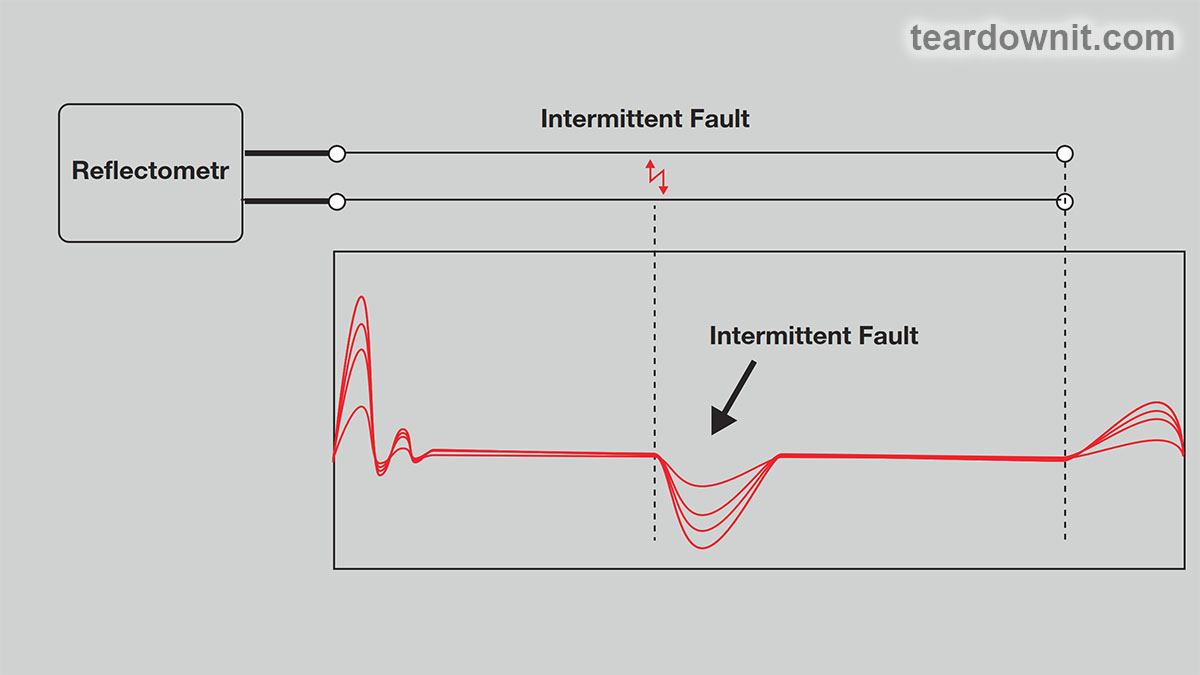 The inconsistent nature of 'floating' defects complicates their localization; it becomes possible only if the data is accumulated over a relatively long period (sometimes up to a day). To solve this problem, some reflectometers implement a special intermittent fault detection function. When activated, the device connected to the line accumulates all reflectograms and displays them overlayed on each other. The 'floating' defect shows up as the difference in graphs. It is enough to connect the device to the line and leave it for the period during which the defect is guaranteed to appear. SEARCHING FOR CROSSED CABLE PAIRS Resolving cross-pairs in structured cabling systems is extremely difficult. Finding them takes much longer than finding any other damage. 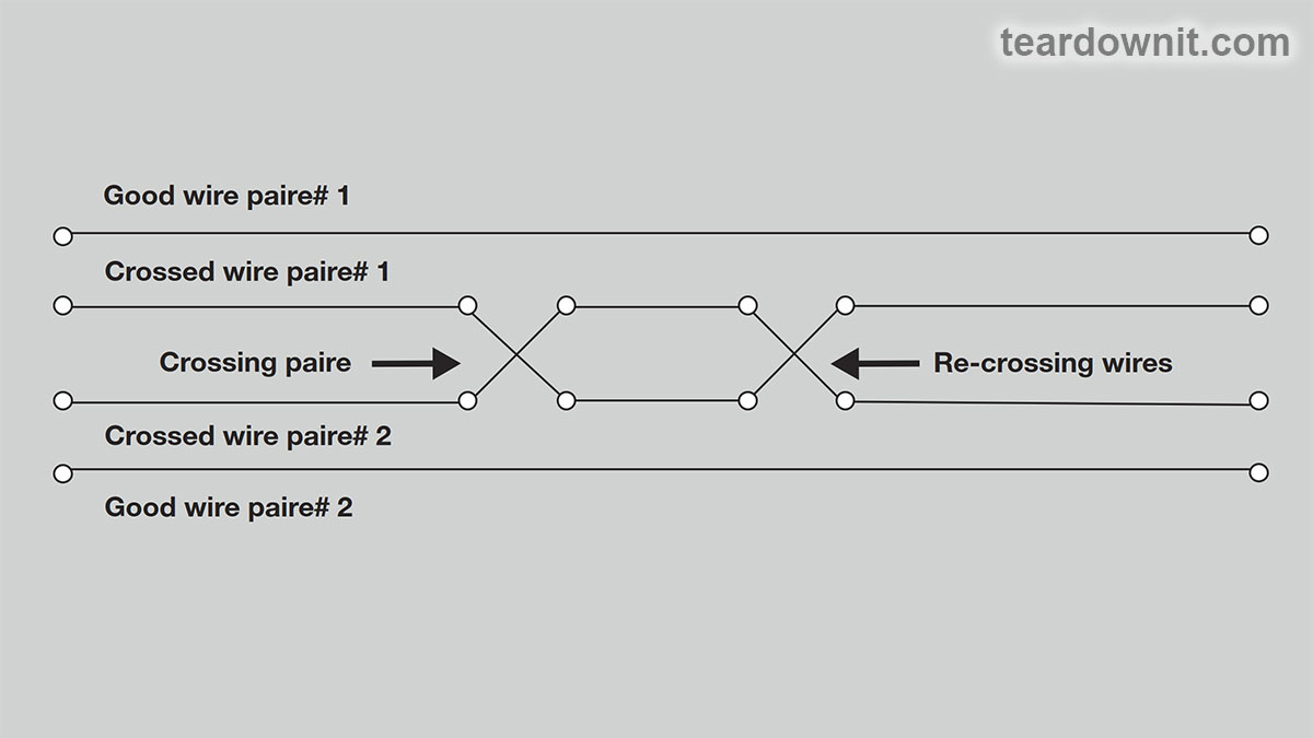 Fixing such damage is much cheaper than replacing the entire cable or laying an additional one. Using an identification tone and an OTDR is one of the simplest methods for quickly and reliably locating tangled wires. First, you should understand the causes and symptoms of the malfunction. We must remember that mixing up wires is a human error. This malfunction appears mainly at cable splices (in couplings) when two wires of the same color but belonging to different pairs are connected. This situation usually results in unacceptable crosstalk. Most often, this happens due to the inconsistency of the twist and the susceptibility of the untwisted cable pair to parasitic signals. As a result, the wires act as antennas. In addition to receiving a strong spurious signal from external sources, the untwisted pair itself has increased radiation and has a negative effect on the remaining pairs in the bundle. The primary way to solve the problem is to fix the defect in the next cable coupling line. We are talking about restoring the correct connection (and, in fact, about re-tangling the same wires). This is the simplest solution, which, of course, does not eliminate the problem. In any case, this section of the cable must be repaired. FINDING THE SPOT OF THE BREAKAGE The instruments used to test cables are often unable to detect mixed pairs. For example, a bridge-type meter turns out to be ineffective. This device combines an AC bridge (capacitive bridge) and a DC bridge (resistive bridge). The capacitive bridge will show a fault in the cable. It will be able to determine the length of the defective section of the cable since the reversed pair has a reduced capacitance. However, it will not allow you to determine the distance to the place where the mix-up occurred. A resistive bridge is unsuitable in this case since mixing up the wires has virtually no effect on their resistance. 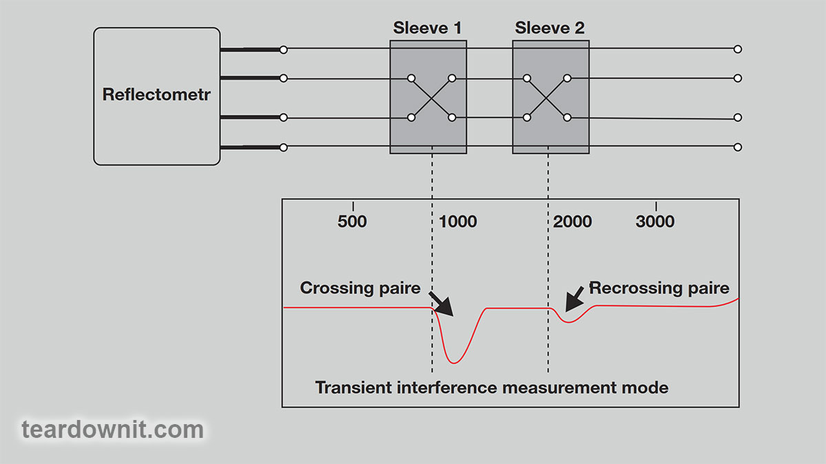 Note that some reflectometer models have a function for sending an identification tone, which greatly facilitates the search for mixed-up cable pairs using a reflectometer. The tone allows you to identify the cable pair that is tangled with the one being tested. It usually belongs to the same cable bundle. 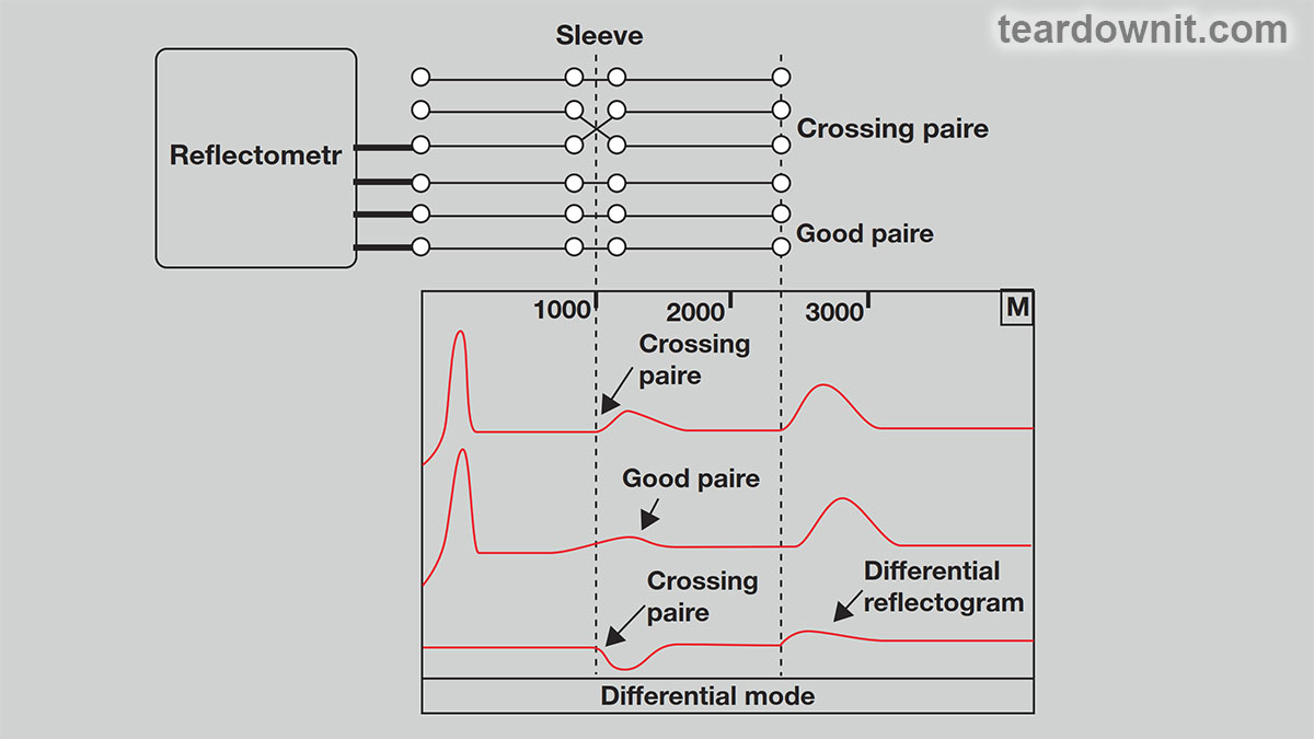 There are two ways to look for places where wires are mixed up. The simplest way is to check the cable using a reflectometer for transient interference. When both tangled pairs are connected to the reflectometer ports, the reflectometer sends a pulse to the tested cable pair. It receives a reflected pulse from the second pair. There is usually a noticeable spike on the display at the point where the wires get tangled. It can be of either positive or negative polarity, which depends on the polarity of connecting the test leads of the reflectometer to the cable cores. 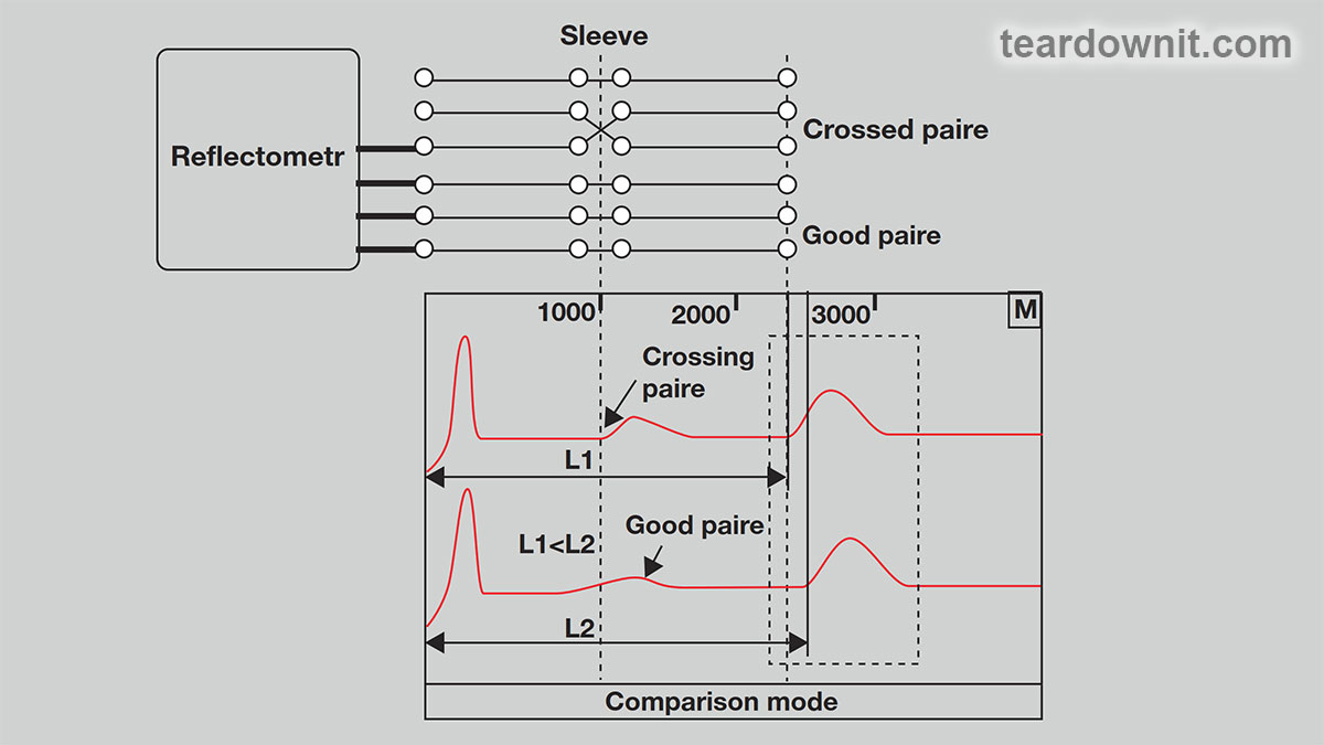 Another method uses the reflectometer in differential or comparison mode when a pair with reversed wires is compared with a known good pair or subtracted from it (in differential mode). A faulty pair will give a higher level of reflection in the cable box in which the wires were mixed up. This is where the highest transient interference occurs. Comparing or subtracting the signals from two tangled cable pairs will not indicate damage to the instrument display. It should be noted that if the open far end of the cable is visible on the reflectogram, then the distance for the tangled cable pair is less than for the "good" pair from the same cable. The mixed-up section has lower capacitance, which means the signal travels faster along it. Consequently, the reflectometer interprets this section of cable as a shorter one. If somewhere the wires are tangled twice (that is, they were first mixed up, and then after some distance, the original pairs were untangled), then first of all, you need to find the place where they are mixed up, and then determine the location of the second switching using any of the two above methods. |
| json metadata | {"tags":["reflectometer"],"image":["https://cdn.steemitimages.com/DQmbhjckmrYZy2xfmpEuhMa8y2XSEMLktZwhHR8ZJT81KaM/image.png","https://cdn.steemitimages.com/DQmaDqps729dKGH1fSRJpUM8qqJHQAZpsyMHiR9EfS8MktX/image.png","https://cdn.steemitimages.com/DQmdTwBJ67jae3DuDCNv5jq7hg4wgXTKQSUtWRx7pQLfQ4b/image.png","https://cdn.steemitimages.com/DQmTHdCVESrAiwUFkRV3SH8TKj6UfxAnVJ294sp9FcCJHeq/image.png","https://cdn.steemitimages.com/DQmXRsDFBgy3tucnooT2dpGX9vXSWGhBrvu6UtxDQDe4qYj/image.png"],"app":"steemit/0.2","format":"markdown"} |
| parent author | |
| parent permlink | reflectometer |
| permlink | reflectometer-applications-methods-for-finding-significant-cable-damage |
| title | Reflectometer applications: methods for finding significant cable damage |
| Transaction Info | Block #82978712/Trx 982491e4ffa7f386a035d2e4b03aae1122692e3f |
View Raw JSON Data
{
"block": 82978712,
"op": [
"comment",
{
"author": "teardownit",
"body": "The primary and most common damage types are wire casing damages or cable installation errors. These typically are 'floating' defects and wire connection errors. Let's learn the technique of searching for those kinds of faults.\n\nAUTOMATIC DEFECT SEARCH\nLet's start with the automatic search mode. This method automatically compares defects detected on the reflectogram with a threshold value of reverse attenuation. The method of automated comparison with a threshold value greatly simplifies reflectogram viewing. If, for example, you set the threshold to 30 dBRL, the reflectometer will automatically display only the faults with a return attenuation value of 30 dBRL or less.\n\nFIXATION OF 'FLOATING' DEFECTS\nLocating 'floating' defects is another indispensable function of a modern reflectometer. Only with its help can it be possible to point out the locations of the periodically repeating effects of weak wire connections or reduced insulation resistance. Defects of this kind manifest themselves in customer complaints about random signal loss. 'Floating' defects can appear for various reasons: when a signal is applied, due to mechanical stress on the cable at the point of damage (for example, vibration from nearby operating equipment like an elevator), etc.\n\n\n\nThe inconsistent nature of 'floating' defects complicates their localization; it becomes possible only if the data is accumulated over a relatively long period (sometimes up to a day). To solve this problem, some reflectometers implement a special intermittent fault detection function. When activated, the device connected to the line accumulates all reflectograms and displays them overlayed on each other. The 'floating' defect shows up as the difference in graphs. It is enough to connect the device to the line and leave it for the period during which the defect is guaranteed to appear.\n\nSEARCHING FOR CROSSED CABLE PAIRS\nResolving cross-pairs in structured cabling systems is extremely difficult. Finding them takes much longer than finding any other damage.\n\n\n\n\n\nFixing such damage is much cheaper than replacing the entire cable or laying an additional one. Using an identification tone and an OTDR is one of the simplest methods for quickly and reliably locating tangled wires.\nFirst, you should understand the causes and symptoms of the malfunction. We must remember that mixing up wires is a human error. This malfunction appears mainly at cable splices (in couplings) when two wires of the same color but belonging to different pairs are connected.\nThis situation usually results in unacceptable crosstalk. Most often, this happens due to the inconsistency of the twist and the susceptibility of the untwisted cable pair to parasitic signals. As a result, the wires act as antennas. In addition to receiving a strong spurious signal from external sources, the untwisted pair itself has increased radiation and has a negative effect on the remaining pairs in the bundle.\nThe primary way to solve the problem is to fix the defect in the next cable coupling line. We are talking about restoring the correct connection (and, in fact, about re-tangling the same wires). This is the simplest solution, which, of course, does not eliminate the problem. In any case, this section of the cable must be repaired.\n\nFINDING THE SPOT OF THE BREAKAGE\nThe instruments used to test cables are often unable to detect mixed pairs. For example, a bridge-type meter turns out to be ineffective. This device combines an AC bridge (capacitive bridge) and a DC bridge (resistive bridge). The capacitive bridge will show a fault in the cable. It will be able to determine the length of the defective section of the cable since the reversed pair has a reduced capacitance. However, it will not allow you to determine the distance to the place where the mix-up occurred. A resistive bridge is unsuitable in this case since mixing up the wires has virtually no effect on their resistance.\n\n\n\nNote that some reflectometer models have a function for sending an identification tone, which greatly facilitates the search for mixed-up cable pairs using a reflectometer. The tone allows you to identify the cable pair that is tangled with the one being tested. It usually belongs to the same cable bundle.\n\n\n\nThere are two ways to look for places where wires are mixed up. The simplest way is to check the cable using a reflectometer for transient interference. When both tangled pairs are connected to the reflectometer ports, the reflectometer sends a pulse to the tested cable pair. It receives a reflected pulse from the second pair. There is usually a noticeable spike on the display at the point where the wires get tangled. It can be of either positive or negative polarity, which depends on the polarity of connecting the test leads of the reflectometer to the cable cores.\n\n\n\nAnother method uses the reflectometer in differential or comparison mode when a pair with reversed wires is compared with a known good pair or subtracted from it (in differential mode). A faulty pair will give a higher level of reflection in the cable box in which the wires were mixed up. This is where the highest transient interference occurs. Comparing or subtracting the signals from two tangled cable pairs will not indicate damage to the instrument display. It should be noted that if the open far end of the cable is visible on the reflectogram, then the distance for the tangled cable pair is less than for the \"good\" pair from the same cable. The mixed-up section has lower capacitance, which means the signal travels faster along it. Consequently, the reflectometer interprets this section of cable as a shorter one.\nIf somewhere the wires are tangled twice (that is, they were first mixed up, and then after some distance, the original pairs were untangled), then first of all, you need to find the place where they are mixed up, and then determine the location of the second switching using any of the two above methods.",
"json_metadata": "{\"tags\":[\"reflectometer\"],\"image\":[\"https://cdn.steemitimages.com/DQmbhjckmrYZy2xfmpEuhMa8y2XSEMLktZwhHR8ZJT81KaM/image.png\",\"https://cdn.steemitimages.com/DQmaDqps729dKGH1fSRJpUM8qqJHQAZpsyMHiR9EfS8MktX/image.png\",\"https://cdn.steemitimages.com/DQmdTwBJ67jae3DuDCNv5jq7hg4wgXTKQSUtWRx7pQLfQ4b/image.png\",\"https://cdn.steemitimages.com/DQmTHdCVESrAiwUFkRV3SH8TKj6UfxAnVJ294sp9FcCJHeq/image.png\",\"https://cdn.steemitimages.com/DQmXRsDFBgy3tucnooT2dpGX9vXSWGhBrvu6UtxDQDe4qYj/image.png\"],\"app\":\"steemit/0.2\",\"format\":\"markdown\"}",
"parent_author": "",
"parent_permlink": "reflectometer",
"permlink": "reflectometer-applications-methods-for-finding-significant-cable-damage",
"title": "Reflectometer applications: methods for finding significant cable damage"
}
],
"op_in_trx": 0,
"timestamp": "2024-03-01T23:52:15",
"trx_id": "982491e4ffa7f386a035d2e4b03aae1122692e3f",
"trx_in_block": 2,
"virtual_op": 0
}teardownitpublished a new post: diy-single-transistor-reflex-am-radio-with-regeneration-and-agc2024/02/22 23:13:18
teardownitpublished a new post: diy-single-transistor-reflex-am-radio-with-regeneration-and-agc
2024/02/22 23:13:18
| author | teardownit |
| body | https://assets-global.website-files.com/6438c93ff266bb9903cab3bc/65cda7c9fc7f1f4752710f02_0.jpg This is a piece of circuitry magic; it's a great pleasure to assemble and configure it! The receiver sounds pretty good if a medium-wave station is nearby or an AM transmitter is at home. In the previous post, we've assembled an eight-transistor AM MW superheterodyne. This is an excellent, straightforward solution for reliable, high-quality radio reception. Still, the scheme is a bit too complex for a beginner. A few decades ago, it was also not budget-friendly; it was three times more expensive than a tube All American Five (midget, peewee) radio. Simpler amateur DIY receivers were more common, using one or two and sometimes up to three transistors. Today, we will assemble and look into one of those schemes.  By the way, if you experiment with vintage tube radios and TVs, remember that many are powered directly from the mains without a transformer. That means the chassis and all components could be under high voltage relative to the ground!  Peewee radios often came with a special power cord called a "line cord resistor." It was a cord with a certain resistance, so the voltage drop across it was a pre-defined value. This cord heated up during operation; it was introduced just to move the heat source outside the small radio housing. https://assets-global.website-files.com/6438c93ff266bb9903cab3bc/65cda7dc85c8103e2cebf537_3.jpg And finally, vintage transformers after long-time sitting may have a winding breakdown, primary to secondary or primary to the magnetic core, which is connected electrically to the chassis. Therefore, before powering on an old electronic device, start by examining its schematics and checking for insulation breakdowns. Make sure you use the correct power cord and the correct arrangement of contacts in the wall plug (chassis to ground); use fuses and breakers. It wouldn't hurt to have an isolation transformer, either. All that being said, let's begin. RF-tuned radios are usually described with the formula number-V-number. The letter V denotes the detector; the first number is the number of RF gain stages, and the second is the number of AF gain stages. Let's take a crystal radio and connect a single-transistor AF amplifier after the detector. The result is a radio receiver 0V1.  Or you can connect the transistor before the detector. Then, the device will amplify the radio frequency and will be called 1V0. It works like this: the amplified RF voltage drops across choke L3, which has a high impedance at high frequency. It is detected (rectified) by a diode, integrated by a capacitor C4, and sent to the earbud.  And here, we have a 0V0 receiver because the transistor in this circuit serves not as an amplifier but as a detector. It operates in such a mode as to amplify only one half-cycle of the input signal, the positive one. The bias resistor R1 is responsible for the transistor mode. L3 and C4 are integrators that convert the energy of high-frequency oscillations into low-frequency ones.  So, we've remembered that capacitors have low impedance for high frequencies and high impedance for low frequencies and do not pass direct current through at all. With inductors, it’s the other way around: they easily pass direct current, have little resistance to low-frequency current, and have strong resistance to high-frequency current. What if we amplify a high-frequency signal from a radio station with a transistor, feed it to a detector, integrate it, and feed it to the input of the same transistor again, this time in the form of a low-frequency audio signal? Surprisingly, it is possible. On a single transistor, we will get ourselves a 1V1 receiver like the 1962 Japanese Lark TR-107. In those years, imported radios with less than three transistors were eligible for customs exemptions when imported into the United States. It was an intelligent decision. On the one hand, it stimulated the domestic production of more complex and advanced receivers. On the other, it made a pocket receiver accessible to everyone so that in the case of an emergency, everyone would receive public warning alerts in no time. Therefore, two seemingly mutually exclusive trends occurred. Manufacturers from Japan were making some of their receivers as advanced as possible using one or two transistors and a pair of diodes to successfully compete in the lower price segment of the US market. On the contrary, other devices used a third transistor simply as a diode to create the cheapest mid-range radios. The same thing was happening in the premium segment. In the last post, we assembled an 8-transistor superheterodyne, where one of the transistors acts as a diode. For the end customer, 8 transistors sounded more prestigious than 7. Replacing a cheap diode with an expensive transistor today seems unreasonable. But let me remind you that poor-quality transistors in a batch were easy to find in those days. Those were picked and used instead of diodes, which was also a saving! I should add that the same marketing increase in active elements occurred in the tube era. Take All American Five, with a sixth lamp added as a ballast resistor. It did not improve the quality of radio reception or sound. But a six-tube radio is more prestigious than a five-tube radio. The substantial benefit of having the sixth lamp was that it made it possible to ditch the line cord resistor, thereby eliminating the suboptimal outcome of setting a curtain on fire. For the line cord resistor to cool down properly, it should not be twisted or covered. Fires were a real threat when this safety requirement was neglected. So, we have a diagram of the 1962 Lark TR-107. The lower end of the secondary winding L1 is grounded at high frequency by capacitor C2. From its upper end, the audio signal enters the base of the transistor and is amplified. https://assets-global.website-files.com/6438c93ff266bb9903cab3bc/65cda7f259aa0e006aa52af3_7.jpg L2 is a high-frequency transformer that is often wound on a ferrite ring. Capacitor C3 and two diodes form a voltage-doubling rectifier, and C2 is its integrator, forming a detector. The low-frequency signal of the detector passes freely through the secondary winding L1 and is amplified by the transistor, then passes freely through the primary winding L2 and enters the primary winding of the matching transformer T, the output of which has an earbud connected to it. The inductance of the winding L2 and the capacitance C3 are small, so the audio frequency signal basically does not reach the detector diodes. Therefore, self-excitation does not occur. Thus, one transistor amplifies both radio and audio frequencies! Such a radio receiver is called reflex, like in "reflection": the signal after the detector is reflected back and again enters the transistor amplifier stage.  The receiver I've put together is based on the iconic Chinese radio "636" design from 1963. Thanks to its clever design, it was a bestseller and is still considered one of the best single-transistor radios. Let's compare it to the 1962 Lark TR-107.  The custom "reflex" transformer was replaced with a simple mass-market RF choke L. This brought down the cost and simplified the assembly without sacrificing quality. The device was sold as a finished product or an assembly kit and was widely available. Over 60 years, the scheme has undergone several improvements. There was a two-transistor version for low-impedance headphones and a three-transistor version with a loudspeaker. Still, these variations altered only the audio path and are insignificant for our study. Let's take a look at improvements to the radio part. First, a positive feedback winding is added between the transistor emitter and the ground. This is a tickler winding, which can significantly increase the receiver's sensitivity. It adds some energy to the weak magnetic antenna signal at the same frequency that the antenna resonant tank is tuned to. This way, a weak signal becomes a strong one. The feedback winding contains no more than two turns, so it does not interfere with amplifying high and low frequencies. The end result was not just a reflexive but a regenerative receiver. If we do not need regeneration, the additional winding can be short-circuited with the jumper JP1. To prevent regeneration from turning into self-excitation, a trimming resistor W is added for gain adjustment. To ensure that a weak signal is amplified more and a strong signal less, there's auto gain control: an integrator consisting of capacitor C4 and resistor R1 selects the amplitude envelope of the detector signal and supplies it to the base of the transistor. Then, LED D1 is not a power-on indicator but a transistor base bias stabilizer. The LED works like a stabilator: the voltage across it is almost independent of the current flowing through it. Thanks to this LED, the gain will not go down as the batteries are used up. And when swapping molten-salt batteries with alkaline ones, the receiver, despite being configured for the former, will not self-excite. Jumper JP2 may be needed to adjust the collector current of the transistor. If there is no input signal, it should equal 1 mA. Open jumper JP3 and close JP4 if we connect not an audio amplifier but an earbud to the radio output. If this is a mono headphone, then open JP5. The video below shows this receiver's assembly and operation. https://youtu.be/4UJyl4f20lQ Thanks for your attention! |
| json metadata | {"tags":["diy"],"image":["https://assets-global.website-files.com/6438c93ff266bb9903cab3bc/65cda7c9fc7f1f4752710f02_0.jpg","https://cdn.steemitimages.com/DQma6HfjBpphzTRDwBVN6f8sJfQLNc6KSe1x1MmBAb4FXve/image.png","https://cdn.steemitimages.com/DQmc5f3WfbDAY82EDYUfZDADAdFajQcFoNkyqNQmFK3dRhK/image.png","https://assets-global.website-files.com/6438c93ff266bb9903cab3bc/65cda7dc85c8103e2cebf537_3.jpg","https://cdn.steemitimages.com/DQmW8iBfM34yk4STMPxMXHsK1omKeWN2bzVxJQgvfrCEgwh/image.png","https://cdn.steemitimages.com/DQmZbfdo2uiRSrFypDPgF2ickoRcWxQG21uWP7TeAya1s2u/image.png","https://cdn.steemitimages.com/DQmR2c7SvyQzusd9XzGphBFB3BL67nF9h6gqcXJETrfPD4D/image.png","https://assets-global.website-files.com/6438c93ff266bb9903cab3bc/65cda7f259aa0e006aa52af3_7.jpg","https://cdn.steemitimages.com/DQmYoZWAh7bBqYrLB6x63rGjW9cow9bPBjrv5CK1e8hJyRn/image.png","https://cdn.steemitimages.com/DQmQFXh8fWHNQGt1QUaLYyiaLRE4Ui8DMEZkLKvnHLZUSDY/image.png","https://img.youtube.com/vi/4UJyl4f20lQ/0.jpg"],"links":["https://youtu.be/4UJyl4f20lQ"],"app":"steemit/0.2","format":"markdown"} |
| parent author | |
| parent permlink | diy |
| permlink | diy-single-transistor-reflex-am-radio-with-regeneration-and-agc |
| title | DIY single transistor reflex AM radio with regeneration and AGC |
| Transaction Info | Block #82748854/Trx 2d699e843449367dd51bc8ed4e2a4a1162523d26 |
View Raw JSON Data
{
"block": 82748854,
"op": [
"comment",
{
"author": "teardownit",
"body": "https://assets-global.website-files.com/6438c93ff266bb9903cab3bc/65cda7c9fc7f1f4752710f02_0.jpg\n\nThis is a piece of circuitry magic; it's a great pleasure to assemble and configure it! The receiver sounds pretty good if a medium-wave station is nearby or an AM transmitter is at home.\n\nIn the previous post, we've assembled an eight-transistor AM MW superheterodyne. This is an excellent, straightforward solution for reliable, high-quality radio reception. Still, the scheme is a bit too complex for a beginner.\n\nA few decades ago, it was also not budget-friendly; it was three times more expensive than a tube All American Five (midget, peewee) radio. Simpler amateur DIY receivers were more common, using one or two and sometimes up to three transistors. Today, we will assemble and look into one of those schemes.\n\n\n\nBy the way, if you experiment with vintage tube radios and TVs, remember that many are powered directly from the mains without a transformer. That means the chassis and all components could be under high voltage relative to the ground!\n\n\n\nPeewee radios often came with a special power cord called a \"line cord resistor.\" It was a cord with a certain resistance, so the voltage drop across it was a pre-defined value. This cord heated up during operation; it was introduced just to move the heat source outside the small radio housing.\n\nhttps://assets-global.website-files.com/6438c93ff266bb9903cab3bc/65cda7dc85c8103e2cebf537_3.jpg\n\nAnd finally, vintage transformers after long-time sitting may have a winding breakdown, primary to secondary or primary to the magnetic core, which is connected electrically to the chassis.\n\nTherefore, before powering on an old electronic device, start by examining its schematics and checking for insulation breakdowns. Make sure you use the correct power cord and the correct arrangement of contacts in the wall plug (chassis to ground); use fuses and breakers. It wouldn't hurt to have an isolation transformer, either.\n\nAll that being said, let's begin. RF-tuned radios are usually described with the formula number-V-number. The letter V denotes the detector; the first number is the number of RF gain stages, and the second is the number of AF gain stages.\n\nLet's take a crystal radio and connect a single-transistor AF amplifier after the detector. The result is a radio receiver 0V1.\n\n\nOr you can connect the transistor before the detector. Then, the device will amplify the radio frequency and will be called 1V0. It works like this: the amplified RF voltage drops across choke L3, which has a high impedance at high frequency. It is detected (rectified) by a diode, integrated by a capacitor C4, and sent to the earbud.\n\n\nAnd here, we have a 0V0 receiver because the transistor in this circuit serves not as an amplifier but as a detector. It operates in such a mode as to amplify only one half-cycle of the input signal, the positive one. The bias resistor R1 is responsible for the transistor mode. L3 and C4 are integrators that convert the energy of high-frequency oscillations into low-frequency ones.\n\n\n\nSo, we've remembered that capacitors have low impedance for high frequencies and high impedance for low frequencies and do not pass direct current through at all.\n\nWith inductors, it’s the other way around: they easily pass direct current, have little resistance to low-frequency current, and have strong resistance to high-frequency current.\n\nWhat if we amplify a high-frequency signal from a radio station with a transistor, feed it to a detector, integrate it, and feed it to the input of the same transistor again, this time in the form of a low-frequency audio signal?\n\nSurprisingly, it is possible. On a single transistor, we will get ourselves a 1V1 receiver like the 1962 Japanese Lark TR-107.\n\nIn those years, imported radios with less than three transistors were eligible for customs exemptions when imported into the United States. It was an intelligent decision. On the one hand, it stimulated the domestic production of more complex and advanced receivers. On the other, it made a pocket receiver accessible to everyone so that in the case of an emergency, everyone would receive public warning alerts in no time.\n\nTherefore, two seemingly mutually exclusive trends occurred. Manufacturers from Japan were making some of their receivers as advanced as possible using one or two transistors and a pair of diodes to successfully compete in the lower price segment of the US market.\n\nOn the contrary, other devices used a third transistor simply as a diode to create the cheapest mid-range radios. The same thing was happening in the premium segment. In the last post, we assembled an 8-transistor superheterodyne, where one of the transistors acts as a diode. For the end customer, 8 transistors sounded more prestigious than 7.\n\nReplacing a cheap diode with an expensive transistor today seems unreasonable. But let me remind you that poor-quality transistors in a batch were easy to find in those days. Those were picked and used instead of diodes, which was also a saving!\n\nI should add that the same marketing increase in active elements occurred in the tube era. Take All American Five, with a sixth lamp added as a ballast resistor. It did not improve the quality of radio reception or sound. But a six-tube radio is more prestigious than a five-tube radio.\n\nThe substantial benefit of having the sixth lamp was that it made it possible to ditch the line cord resistor, thereby eliminating the suboptimal outcome of setting a curtain on fire. For the line cord resistor to cool down properly, it should not be twisted or covered. Fires were a real threat when this safety requirement was neglected.\n\nSo, we have a diagram of the 1962 Lark TR-107. The lower end of the secondary winding L1 is grounded at high frequency by capacitor C2. From its upper end, the audio signal enters the base of the transistor and is amplified.\nhttps://assets-global.website-files.com/6438c93ff266bb9903cab3bc/65cda7f259aa0e006aa52af3_7.jpg\nL2 is a high-frequency transformer that is often wound on a ferrite ring. Capacitor C3 and two diodes form a voltage-doubling rectifier, and C2 is its integrator, forming a detector.\n\nThe low-frequency signal of the detector passes freely through the secondary winding L1 and is amplified by the transistor, then passes freely through the primary winding L2 and enters the primary winding of the matching transformer T, the output of which has an earbud connected to it.\n\nThe inductance of the winding L2 and the capacitance C3 are small, so the audio frequency signal basically does not reach the detector diodes. Therefore, self-excitation does not occur.\n\nThus, one transistor amplifies both radio and audio frequencies! Such a radio receiver is called reflex, like in \"reflection\": the signal after the detector is reflected back and again enters the transistor amplifier stage.\n\n\n\nThe receiver I've put together is based on the iconic Chinese radio \"636\" design from 1963. Thanks to its clever design, it was a bestseller and is still considered one of the best single-transistor radios. Let's compare it to the 1962 Lark TR-107.\n\n\nThe custom \"reflex\" transformer was replaced with a simple mass-market RF choke L. This brought down the cost and simplified the assembly without sacrificing quality. The device was sold as a finished product or an assembly kit and was widely available.\n\nOver 60 years, the scheme has undergone several improvements. There was a two-transistor version for low-impedance headphones and a three-transistor version with a loudspeaker. Still, these variations altered only the audio path and are insignificant for our study. Let's take a look at improvements to the radio part.\n\nFirst, a positive feedback winding is added between the transistor emitter and the ground. This is a tickler winding, which can significantly increase the receiver's sensitivity.\n\nIt adds some energy to the weak magnetic antenna signal at the same frequency that the antenna resonant tank is tuned to. This way, a weak signal becomes a strong one.\n\nThe feedback winding contains no more than two turns, so it does not interfere with amplifying high and low frequencies.\n\nThe end result was not just a reflexive but a regenerative receiver. If we do not need regeneration, the additional winding can be short-circuited with the jumper JP1.\n\nTo prevent regeneration from turning into self-excitation, a trimming resistor W is added for gain adjustment.\n\nTo ensure that a weak signal is amplified more and a strong signal less, there's auto gain control: an integrator consisting of capacitor C4 and resistor R1 selects the amplitude envelope of the detector signal and supplies it to the base of the transistor.\n\nThen, LED D1 is not a power-on indicator but a transistor base bias stabilizer. The LED works like a stabilator: the voltage across it is almost independent of the current flowing through it.\n\nThanks to this LED, the gain will not go down as the batteries are used up. And when swapping molten-salt batteries with alkaline ones, the receiver, despite being configured for the former, will not self-excite.\n\nJumper JP2 may be needed to adjust the collector current of the transistor. If there is no input signal, it should equal 1 mA.\n\nOpen jumper JP3 and close JP4 if we connect not an audio amplifier but an earbud to the radio output. If this is a mono headphone, then open JP5.\n\nThe video below shows this receiver's assembly and operation.\nhttps://youtu.be/4UJyl4f20lQ\nThanks for your attention!",
"json_metadata": "{\"tags\":[\"diy\"],\"image\":[\"https://assets-global.website-files.com/6438c93ff266bb9903cab3bc/65cda7c9fc7f1f4752710f02_0.jpg\",\"https://cdn.steemitimages.com/DQma6HfjBpphzTRDwBVN6f8sJfQLNc6KSe1x1MmBAb4FXve/image.png\",\"https://cdn.steemitimages.com/DQmc5f3WfbDAY82EDYUfZDADAdFajQcFoNkyqNQmFK3dRhK/image.png\",\"https://assets-global.website-files.com/6438c93ff266bb9903cab3bc/65cda7dc85c8103e2cebf537_3.jpg\",\"https://cdn.steemitimages.com/DQmW8iBfM34yk4STMPxMXHsK1omKeWN2bzVxJQgvfrCEgwh/image.png\",\"https://cdn.steemitimages.com/DQmZbfdo2uiRSrFypDPgF2ickoRcWxQG21uWP7TeAya1s2u/image.png\",\"https://cdn.steemitimages.com/DQmR2c7SvyQzusd9XzGphBFB3BL67nF9h6gqcXJETrfPD4D/image.png\",\"https://assets-global.website-files.com/6438c93ff266bb9903cab3bc/65cda7f259aa0e006aa52af3_7.jpg\",\"https://cdn.steemitimages.com/DQmYoZWAh7bBqYrLB6x63rGjW9cow9bPBjrv5CK1e8hJyRn/image.png\",\"https://cdn.steemitimages.com/DQmQFXh8fWHNQGt1QUaLYyiaLRE4Ui8DMEZkLKvnHLZUSDY/image.png\",\"https://img.youtube.com/vi/4UJyl4f20lQ/0.jpg\"],\"links\":[\"https://youtu.be/4UJyl4f20lQ\"],\"app\":\"steemit/0.2\",\"format\":\"markdown\"}",
"parent_author": "",
"parent_permlink": "diy",
"permlink": "diy-single-transistor-reflex-am-radio-with-regeneration-and-agc",
"title": "DIY single transistor reflex AM radio with regeneration and AGC"
}
],
"op_in_trx": 0,
"timestamp": "2024-02-22T23:13:18",
"trx_id": "2d699e843449367dd51bc8ed4e2a4a1162523d26",
"trx_in_block": 0,
"virtual_op": 0
}bluesnipersent 0.010 STEEM to @teardownit- "Hello. Good to see you on Steem. To maximize your rewards, publish your post also on Hive ( hive.blog ) and Blurt ( blurt.blog ) blockchains. Use upvu, jsup or ctime and get instant upvotes"2024/02/21 22:35:30
bluesnipersent 0.010 STEEM to @teardownit- "Hello. Good to see you on Steem. To maximize your rewards, publish your post also on Hive ( hive.blog ) and Blurt ( blurt.blog ) blockchains. Use upvu, jsup or ctime and get instant upvotes"
2024/02/21 22:35:30
| amount | 0.010 STEEM |
| from | bluesniper |
| memo | Hello. Good to see you on Steem. To maximize your rewards, publish your post also on Hive ( hive.blog ) and Blurt ( blurt.blog ) blockchains. Use upvu, jsup or ctime and get instant upvotes |
| to | teardownit |
| Transaction Info | Block #82719417/Trx d777d3e7be7e111777165f6b307347c8a0afa11b |
View Raw JSON Data
{
  "block": 82719417,
  "op": [
    "transfer",
    {
      "amount": "0.010 STEEM",
      "from": "bluesniper",
      "memo": "Hello. Good to see you on Steem. To maximize your rewards, publish your post also on Hive ( hive.blog ) and Blurt ( blurt.blog ) blockchains. Use upvu, jsup or ctime and get instant upvotes",
      "to": "teardownit"
    }
  ],
  "op_in_trx": 0,
  "timestamp": "2024-02-21T22:35:30",
  "trx_id": "d777d3e7be7e111777165f6b307347c8a0afa11b",
  "trx_in_block": 0,
  "virtual_op": 0
}2024/02/21 22:35:06
2024/02/21 22:35:06
| author | teardownit |
| permlink | review-teardown-and-testing-of-lrs-150-24-mean-well-power-supply |
| voter | bluesniper |
| weight | 10000 (100.00%) |
| Transaction Info | Block #82719409/Trx fc23dae79f9087421ac053f31a895152c0055ebb |
View Raw JSON Data
{
  "block": 82719409,
  "op": [
    "vote",
    {
      "author": "teardownit",
      "permlink": "review-teardown-and-testing-of-lrs-150-24-mean-well-power-supply",
      "voter": "bluesniper",
      "weight": 10000
    }
  ],
  "op_in_trx": 0,
  "timestamp": "2024-02-21T22:35:06",
  "trx_id": "fc23dae79f9087421ac053f31a895152c0055ebb",
  "trx_in_block": 13,
  "virtual_op": 0
}teardownitpublished a new post: review-teardown-and-testing-of-lrs-150-24-mean-well-power-supply2024/02/21 22:29:48
teardownitpublished a new post: review-teardown-and-testing-of-lrs-150-24-mean-well-power-supply
2024/02/21 22:29:48
| author | teardownit |
| body | https://assets-global.website-files.com/6438c93ff266bb9903cab3bc/65ca1e37d46b70780c874c6b_1.jpg The LRS-150-24 power supply can operate from a 100–120 volt or 200–240 volt AC network. The manufacturer states it provides an output current of up to 6.5 amperes at 24 volts. The supply measures 5¾ × 3¾ × 1¼ inches (145 × 95 × 30 millimeters), made on a fiberglass printed circuit board fixed to the base's case. The top cover is perforated in a honeycomb pattern. The case and cover are both made of aluminum. The board is put together neatly, with no visible defects. The components are arranged evenly, and soldering was done with a no-clean flux. Absolutely nothing dangles or rattles in the assembly. No noises of any sort were noticed during the operation of the power supply. The power supply uses a flyback circuit without PFC. https://assets-global.website-files.com/6438c93ff266bb9903cab3bc/65ca1e98608f497dc6ad6a73_b1.jpg The input voltage is supplied to the input node: RF interference filter (1), a pulse surge limiter (varistor), then the voltage goes to the diode bridge (2) and two input electrolytic capacitors (3). The input voltage selector is also located here. Flyback, built on a MW03A controller (4, installed on the back side of the board) and a power switch (5) on a N-channel MOSFET transistor MMF60R290P. Unfortunately, there is no information about the controller on the Internet. The transistor has a channel resistance of 0.29 ohms at 650 volts and 13 amps. The transformer (6) is entirely covered by the casing, so it is unclear what core material is used. The output rectifier (7) is built using a Schottky diode HBR20150 in a TO-220F package screwed to the side wall and covered with casing. It is basically dual 150V 10A diodes connected in parallel. After the diode there are four output electrolytic capacitors (8) and an additional LC filter. Here (12), there is a small output voltage indicator (green LED) and a regulator (tuning resistor) for adjusting the output voltage. Input and output circuits are connected through a shared screw 7-terminal block (10). 3 terminals for the input line, neutral, and ground wires, and 2 in parallel for common and +24V output. The main electrolytic capacitors are designed for operating temperatures up to 220°F (105°C), Rubycon. Two optocouplers (11) are installed in the feedback circuit, most likely with phototransistors transmitting control signals from the low-voltage output to the high-voltage input side. The board has a few cutouts to increase the dielectric strength between the high-voltage and low-voltage sides of the circuit. The picture shows that the board has three unused spots for storage output capacitors (8), most likely used in the other power supplies of the same series but with different output voltages. Test conditions Most tests use metering circuit #1 (see appendices) at 80°F (27°C), 70% relative humidity, and 29.8 inHg pressure. The measurements were performed without preheating the power supply with a short-term load unless mentioned otherwise. The following values were used to determine the load level: https://assets-global.website-files.com/6438c93ff266bb9903cab3bc/65cb07eaecf170690a899413_table1.jpg Output voltage under a constant load https://assets-global.website-files.com/6438c93ff266bb9903cab3bc/65cb07f2f50ec10cfb5763c7_table2.jpg The high stability of the output voltage should be noted. >Power-on parameters Powering on at 100% load The power supply is turned off at least 5 minutes before the test, with a 100% load connected. The oscillogram of switching to a 100% load is shown below (channel 1 is the output voltage, and channel 2 is the current consumption from the grid) https://assets-global.website-files.com/6438c93ff266bb9903cab3bc/65ca1d3aff66b3e5cfa449d2_2.jpg The picture shows three distinguishable phases of the power-on process: - The pulse of the input current charging the input capacitors when connected to the grid has an amplitude of about 7.5 A and a duration of 2 ms. - Waiting for the power supply control circuit to start for about 100 ms. - (Output Voltage Rise Time) Starting the converter, increasing the output voltage, and entering the operating mode) is 8 ms. (Turn On Delay Time) The entire process of entering the operating mode from the moment of powering on) is 119 ms. (Output Voltage Overshoot) Output voltage overshoot is absent; the switching process is aperiodic. >Powering on at 0% load The power supply is turned off at least 5 minutes before the test, with a 100% load connected. Then, the load is disconnected, and the power supply is switched on. The oscillogram of switching to a 0% load is shown below: https://assets-global.website-files.com/6438c93ff266bb9903cab3bc/65ca1f9ffb777eb8145928f7_3.jpg The picture shows three distinguishable phases of the power-on process: The pulse of the input current charging the input capacitors when connected to the grid has an amplitude of about 7 A and a duration of 2 ms. Waiting for the power supply control circuit to start for about 103 ms. (Output Voltage Rise Time) Starting the converter, increasing the output voltage, and entering the operating mode) is 8 ms. (Turn On Delay Time) The entire process of entering the operating mode from the moment of powering on) is 111 ms. (Output Voltage Overshoot) Output voltage overshoot is absent; the switching process is aperiodic. Power-off parameters The power supply was turned off at 100% load, and the input voltage was nominal at the moment of powering off. The oscillogram of the shutdown process is shown below:  The picture shows two phases of the shutdown process: (Shut Down Hold Up Time) The supply continues to operate due to the input capacitors holding charge until the voltage across them drops to a certain critical level at which maintaining the output voltage at the nominal level becomes impossible is 31 ms. (Output Voltage Fall Time) Reduction of the output voltage, stopping voltage conversion, and accelerating the voltage drop is 21 ms. (Output Voltage Undershoot) Output voltage undershoot is absent, and the shutdown process is aperiodic. >Ripple voltage and current 100% load The diagram of the current draw from the grid at 100% load is shown in the oscillogram below. The amplitude of the current is about 7.5 A: https://assets-global.website-files.com/6438c93ff266bb9903cab3bc/65ca1fc0b7af1e666d8df0b3_5.jpg Low-frequency output voltage ripple is under 30 mV (see the oscillogram below): https://assets-global.website-files.com/6438c93ff266bb9903cab3bc/65ca2126db875393ecf173da_6.jpg Output voltage ripple at the converter frequency is under 30 mV (see the oscillogram below): https://assets-global.website-files.com/6438c93ff266bb9903cab3bc/65ca212df7f87d37ecb4e117_7.jpg 75% load Output voltage ripple at the converter frequency is under 30 mV (see the oscillogram below): https://assets-global.website-files.com/6438c93ff266bb9903cab3bc/65ca2140b931cdebe3bfd95e_8.jpg Low-frequency output voltage ripple is under 30 mV (see the oscillogram below): https://assets-global.website-files.com/6438c93ff266bb9903cab3bc/65ca214714ba058954c4256f_9.jpg 50% load Output voltage ripple at the converter frequency stays below 10 mV; see the oscillogram (11): https://assets-global.website-files.com/6438c93ff266bb9903cab3bc/65ca215248d18803b520e9d9_10.jpg https://assets-global.website-files.com/6438c93ff266bb9903cab3bc/65ca2158fac437c9bce76a5d_11.jpg 10% load https://assets-global.website-files.com/6438c93ff266bb9903cab3bc/65ca21617c28fed1c22517eb_12.jpg https://assets-global.website-files.com/6438c93ff266bb9903cab3bc/65ca2167ab768c8e0239a6ba_13.jpg 0% load No-load current consumption was measured with a multimeter, which is 60 mA RMS. (Power Consumption) The first assumption of excessive standby power draw of more than 7 W is wrong since the current in this mode is predominantly reactive. Indeed, the input filter in the circuit contains two capacitors with a capacitance of 0.68 μF each; these low-frequency capacitors are connected in parallel, i.e., an equivalent capacitance of 1.36 μF is connected to the input terminals. A simple calculation shows that the current through these capacitors should be equal to Ic=120×2×pi×60×1.36e-6=61.5 mA. A slight difference from the measured value can be explained by the deviation of the actual parameters from their nominal values and measurement error. Measuring the exact active power consumption at a 0% load with a basic set of instruments (oscilloscope, multimeter, etc.) is impossible. Output voltage ripple at the converter frequency is under 20 mV (see the oscillogram below): https://assets-global.website-files.com/6438c93ff266bb9903cab3bc/65ca2171db875393ecf19a27_14.jpg The amplitude of low-frequency output voltage ripples is about 25 mV (see the oscillogram below): https://assets-global.website-files.com/6438c93ff266bb9903cab3bc/65ca2178b42e253a47bb7e27_15.jpg >Dynamic characteristics A mode with periodic switching between 50% and 100% load was used to evaluate the dynamic characteristics. The process oscillogram is shown below (17): https://assets-global.website-files.com/6438c93ff266bb9903cab3bc/65ca217f23164652ea81ed8d_16.jpg It is evident that the supply’s response to loading changes is close to aperiodic, and there is no overshoot, which indicates a good stability margin. The magnitude of the response to load changes is within 200 mV. Overload protection The claimed protection type is "hiccup mode, recovers automatically after fault condition is removed". This was confirmed during testing. When a short circuit occurs, the power supply periodically tries to turn back on and, if the overload is still present, turns off again until the next attempt. This operating mode reduces energy losses and heating during overload. Still, it does not allow the parallel connection of multiple power supplies with a common output. The output current for the overload protection to kick in is 8.5 A. Input circuit safety assessment (Input discharge) Safety assessment is based on the discharge time constant of the input circuits when disconnected from the grid; the value is 0.384 s. This means that when operating on a 120 V input voltage, the time required to discharge the input circuits to safe values (<42 V) will be 0.61 s: https://assets-global.website-files.com/6438c93ff266bb9903cab3bc/65ca21882a5e864de9a3fc3d_f1.jpg Important: The result is valid for this particular power supply unit; it was obtained for testing purposes and should not be taken as a safety guarantee. Thermal modes When operating with no load connected, no component overheating had been noticed. When operating under load, the input diode bridge heats up most noticeably. With a load of 90% and the top cover closed, the case heats up to approximately 200°F; the hottest spot is located in the area of the diode bridge rectifier. With a load of 95% and the lid closed, the case temperature reaches 230°F: https://assets-global.website-files.com/6438c93ff266bb9903cab3bc/65ca219446bd04e9de1c6571_17.jpg The temperature of the bridge rectifier itself is a dangerous 250°F: https://assets-global.website-files.com/6438c93ff266bb9903cab3bc/65ca219b9139af519f8a465c_18.jpg Somewhere around these load values, the power supply goes into a pulse-power-limiting mode and remains in this state either until the load drops or until it cools down. Then this 'heat up', 'limit power', 'cool down', and 'turn back on' cycle repeats. Other things to consider: Hot summer weather will decrease the maximum sustainable power output this supply can provide even more. The tests were conducted with unobstructed air access to the housing for cooling; any changes may increase the heating. This means that the power supply cannot handle its rated load for a prolonged period with no forced ventilation, and the load should be limited to 5.5 or even 5.0 A. Conclusions The reviewed power supply unit has characteristics generally consistent with those declared by the manufacturer, except for the long-term output power, which should be around 120 W. The build quality is decent; no components clearly unsuitable for the general application, power draw, current, voltage, or temperature were found in the circuit. The stability of the output voltage should be especially noted. |
| json metadata | {"tags":["teardown"],"image":["https://assets-global.website-files.com/6438c93ff266bb9903cab3bc/65ca1e37d46b70780c874c6b_1.jpg","https://assets-global.website-files.com/6438c93ff266bb9903cab3bc/65ca1e98608f497dc6ad6a73_b1.jpg","https://assets-global.website-files.com/6438c93ff266bb9903cab3bc/65cb07eaecf170690a899413_table1.jpg","https://assets-global.website-files.com/6438c93ff266bb9903cab3bc/65cb07f2f50ec10cfb5763c7_table2.jpg","https://assets-global.website-files.com/6438c93ff266bb9903cab3bc/65ca1d3aff66b3e5cfa449d2_2.jpg","https://assets-global.website-files.com/6438c93ff266bb9903cab3bc/65ca1f9ffb777eb8145928f7_3.jpg","https://cdn.steemitimages.com/DQmNYToNHr1X5DUoNKMDsvZ5TnAqiwr2syPSYJX4LnNVYa6/image.png","https://assets-global.website-files.com/6438c93ff266bb9903cab3bc/65ca1fc0b7af1e666d8df0b3_5.jpg","https://assets-global.website-files.com/6438c93ff266bb9903cab3bc/65ca2126db875393ecf173da_6.jpg","https://assets-global.website-files.com/6438c93ff266bb9903cab3bc/65ca212df7f87d37ecb4e117_7.jpg","https://assets-global.website-files.com/6438c93ff266bb9903cab3bc/65ca2140b931cdebe3bfd95e_8.jpg","https://assets-global.website-files.com/6438c93ff266bb9903cab3bc/65ca214714ba058954c4256f_9.jpg","https://assets-global.website-files.com/6438c93ff266bb9903cab3bc/65ca215248d18803b520e9d9_10.jpg","https://assets-global.website-files.com/6438c93ff266bb9903cab3bc/65ca2158fac437c9bce76a5d_11.jpg","https://assets-global.website-files.com/6438c93ff266bb9903cab3bc/65ca21617c28fed1c22517eb_12.jpg","https://assets-global.website-files.com/6438c93ff266bb9903cab3bc/65ca2167ab768c8e0239a6ba_13.jpg","https://assets-global.website-files.com/6438c93ff266bb9903cab3bc/65ca2171db875393ecf19a27_14.jpg","https://assets-global.website-files.com/6438c93ff266bb9903cab3bc/65ca2178b42e253a47bb7e27_15.jpg","https://assets-global.website-files.com/6438c93ff266bb9903cab3bc/65ca217f23164652ea81ed8d_16.jpg","https://assets-global.website-files.com/6438c93ff266bb9903cab3bc/65ca21882a5e864de9a3fc3d_f1.jpg","https://assets-global.website-files.com/6438c93ff266bb9903cab3bc/65ca219446bd04e9de1c6571_17.jpg","https://assets-global.website-files.com/6438c93ff266bb9903cab3bc/65ca219b9139af519f8a465c_18.jpg"],"app":"steemit/0.2","format":"markdown"} |
| parent author | |
| parent permlink | teardown |
| permlink | review-teardown-and-testing-of-lrs-150-24-mean-well-power-supply |
| title | Review, teardown, and testing of LRS-150-24 Mean Well power supply |
| Transaction Info | Block #82719304/Trx 751b64a52ab268d1081dc187a4796207e2776f10 |
View Raw JSON Data
{
"block": 82719304,
"op": [
"comment",
{
"author": "teardownit",
"body": "https://assets-global.website-files.com/6438c93ff266bb9903cab3bc/65ca1e37d46b70780c874c6b_1.jpg\n\nThe LRS-150-24 power supply can operate from a 100–120 volt or 200–240 volt AC network. The manufacturer states it provides an output current of up to 6.5 amperes at 24 volts. The supply measures 5¾ × 3¾ × 1¼ inches (145 × 95 × 30 millimeters), made on a fiberglass printed circuit board fixed to the base's case. The top cover is perforated in a honeycomb pattern. The case and cover are both made of aluminum.\n\nThe board is put together neatly, with no visible defects. The components are arranged evenly, and soldering was done with a no-clean flux. Absolutely nothing dangles or rattles in the assembly.\n\nNo noises of any sort were noticed during the operation of the power supply.\n\nThe power supply uses a flyback circuit without PFC.\n\nhttps://assets-global.website-files.com/6438c93ff266bb9903cab3bc/65ca1e98608f497dc6ad6a73_b1.jpg\nThe input voltage is supplied to the input node: RF interference filter (1), a pulse surge limiter (varistor), then the voltage goes to the diode bridge (2) and two input electrolytic capacitors (3). The input voltage selector is also located here. Flyback, built on a MW03A controller (4, installed on the back side of the board) and a power switch (5) on a N-channel MOSFET transistor MMF60R290P. Unfortunately, there is no information about the controller on the Internet. The transistor has a channel resistance of 0.29 ohms at 650 volts and 13 amps. The transformer (6) is entirely covered by the casing, so it is unclear what core material is used. The output rectifier (7) is built using a Schottky diode HBR20150 in a TO-220F package screwed to the side wall and covered with casing. It is basically dual 150V 10A diodes connected in parallel. After the diode there are four output electrolytic capacitors (8) and an additional LC filter. Here (12), there is a small output voltage indicator (green LED) and a regulator (tuning resistor) for adjusting the output voltage. Input and output circuits are connected through a shared screw 7-terminal block (10). 3 terminals for the input line, neutral, and ground wires, and 2 in parallel for common and +24V output.\n\nThe main electrolytic capacitors are designed for operating temperatures up to 220°F (105°C), Rubycon. Two optocouplers (11) are installed in the feedback circuit, most likely with phototransistors transmitting control signals from the low-voltage output to the high-voltage input side.\n\nThe board has a few cutouts to increase the dielectric strength between the high-voltage and low-voltage sides of the circuit.\n\nThe picture shows that the board has three unused spots for storage output capacitors (8), most likely used in the other power supplies of the same series but with different output voltages.\n\nTest conditions\nMost tests use metering circuit #1 (see appendices) at 80°F (27°C), 70% relative humidity, and 29.8 inHg pressure.\n\nThe measurements were performed without preheating the power supply with a short-term load unless mentioned otherwise.\n\nThe following values were used to determine the load level:\n\nhttps://assets-global.website-files.com/6438c93ff266bb9903cab3bc/65cb07eaecf170690a899413_table1.jpg\n\nOutput voltage under a constant load\nhttps://assets-global.website-files.com/6438c93ff266bb9903cab3bc/65cb07f2f50ec10cfb5763c7_table2.jpg\nThe high stability of the output voltage should be noted.\n\n>Power-on parameters\nPowering on at 100% load\nThe power supply is turned off at least 5 minutes before the test, with a 100% load connected.\n\nThe oscillogram of switching to a 100% load is shown below (channel 1 is the output voltage, and channel 2 is the current consumption from the grid)\nhttps://assets-global.website-files.com/6438c93ff266bb9903cab3bc/65ca1d3aff66b3e5cfa449d2_2.jpg\n\nThe picture shows three distinguishable phases of the power-on process:\n\n- The pulse of the input current charging the input capacitors when connected to the grid has an amplitude of about 7.5 A and a duration of 2 ms.\n- Waiting for the power supply control circuit to start for about 100 ms.\n- (Output Voltage Rise Time) Starting the converter, increasing the output voltage, and entering the operating mode) is 8 ms.\n(Turn On Delay Time) The entire process of entering the operating mode from the moment of powering on) is 119 ms.\n\n(Output Voltage Overshoot) Output voltage overshoot is absent; the switching process is aperiodic.\n\n>Powering on at 0% load\nThe power supply is turned off at least 5 minutes before the test, with a 100% load connected. Then, the load is disconnected, and the power supply is switched on.\n\nThe oscillogram of switching to a 0% load is shown below:\n\nhttps://assets-global.website-files.com/6438c93ff266bb9903cab3bc/65ca1f9ffb777eb8145928f7_3.jpg\nThe picture shows three distinguishable phases of the power-on process:\n\nThe pulse of the input current charging the input capacitors when connected to the grid has an amplitude of about 7 A and a duration of 2 ms.\nWaiting for the power supply control circuit to start for about 103 ms.\n(Output Voltage Rise Time) Starting the converter, increasing the output voltage, and entering the operating mode) is 8 ms.\n(Turn On Delay Time) The entire process of entering the operating mode from the moment of powering on) is 111 ms.\n\n(Output Voltage Overshoot) Output voltage overshoot is absent; the switching process is aperiodic.\n\nPower-off parameters\nThe power supply was turned off at 100% load, and the input voltage was nominal at the moment of powering off. The oscillogram of the shutdown process is shown below:\n\n\n\nThe picture shows two phases of the shutdown process:\n\n(Shut Down Hold Up Time) The supply continues to operate due to the input capacitors holding charge until the voltage across them drops to a certain critical level at which maintaining the output voltage at the nominal level becomes impossible is 31 ms.\n\n(Output Voltage Fall Time) Reduction of the output voltage, stopping voltage conversion, and accelerating the voltage drop is 21 ms.\n\n(Output Voltage Undershoot) Output voltage undershoot is absent, and the shutdown process is aperiodic.\n\n>Ripple voltage and current\n\n100% load\nThe diagram of the current draw from the grid at 100% load is shown in the oscillogram below. The amplitude of the current is about 7.5 A:\nhttps://assets-global.website-files.com/6438c93ff266bb9903cab3bc/65ca1fc0b7af1e666d8df0b3_5.jpg\nLow-frequency output voltage ripple is under 30 mV (see the oscillogram below):\n\nhttps://assets-global.website-files.com/6438c93ff266bb9903cab3bc/65ca2126db875393ecf173da_6.jpg\nOutput voltage ripple at the converter frequency is under 30 mV (see the oscillogram below):\n\nhttps://assets-global.website-files.com/6438c93ff266bb9903cab3bc/65ca212df7f87d37ecb4e117_7.jpg\n\n75% load\nOutput voltage ripple at the converter frequency is under 30 mV (see the oscillogram below):\nhttps://assets-global.website-files.com/6438c93ff266bb9903cab3bc/65ca2140b931cdebe3bfd95e_8.jpg\n\nLow-frequency output voltage ripple is under 30 mV (see the oscillogram below):\nhttps://assets-global.website-files.com/6438c93ff266bb9903cab3bc/65ca214714ba058954c4256f_9.jpg\n\n50% load\nOutput voltage ripple at the converter frequency stays below 10 mV; see the oscillogram (11):\nhttps://assets-global.website-files.com/6438c93ff266bb9903cab3bc/65ca215248d18803b520e9d9_10.jpg\nhttps://assets-global.website-files.com/6438c93ff266bb9903cab3bc/65ca2158fac437c9bce76a5d_11.jpg\n\n10% load\nhttps://assets-global.website-files.com/6438c93ff266bb9903cab3bc/65ca21617c28fed1c22517eb_12.jpg\nhttps://assets-global.website-files.com/6438c93ff266bb9903cab3bc/65ca2167ab768c8e0239a6ba_13.jpg\n\n0% load\nNo-load current consumption was measured with a multimeter, which is 60 mA RMS.\n\n(Power Consumption) The first assumption of excessive standby power draw of more than 7 W is wrong since the current in this mode is predominantly reactive. Indeed, the input filter in the circuit contains two capacitors with a capacitance of 0.68 μF each; these low-frequency capacitors are connected in parallel, i.e., an equivalent capacitance of 1.36 μF is connected to the input terminals. A simple calculation shows that the current through these capacitors should be equal to Ic=120×2×pi×60×1.36e-6=61.5 mA. A slight difference from the measured value can be explained by the deviation of the actual parameters from their nominal values and measurement error.\n\nMeasuring the exact active power consumption at a 0% load with a basic set of instruments (oscilloscope, multimeter, etc.) is impossible.\n\nOutput voltage ripple at the converter frequency is under 20 mV (see the oscillogram below):\n\nhttps://assets-global.website-files.com/6438c93ff266bb9903cab3bc/65ca2171db875393ecf19a27_14.jpg\nThe amplitude of low-frequency output voltage ripples is about 25 mV (see the oscillogram below):\n\nhttps://assets-global.website-files.com/6438c93ff266bb9903cab3bc/65ca2178b42e253a47bb7e27_15.jpg\n\n>Dynamic characteristics\nA mode with periodic switching between 50% and 100% load was used to evaluate the dynamic characteristics. The process oscillogram is shown below (17):\nhttps://assets-global.website-files.com/6438c93ff266bb9903cab3bc/65ca217f23164652ea81ed8d_16.jpg\n\nIt is evident that the supply’s response to loading changes is close to aperiodic, and there is no overshoot, which indicates a good stability margin. The magnitude of the response to load changes is within 200 mV.\n\nOverload protection\n\nThe claimed protection type is \"hiccup mode, recovers automatically after fault condition is removed\". This was confirmed during testing. When a short circuit occurs, the power supply periodically tries to turn back on and, if the overload is still present, turns off again until the next attempt. This operating mode reduces energy losses and heating during overload. Still, it does not allow the parallel connection of multiple power supplies with a common output.\n\nThe output current for the overload protection to kick in is 8.5 A.\n\nInput circuit safety assessment\n(Input discharge) Safety assessment is based on the discharge time constant of the input circuits when disconnected from the grid; the value is 0.384 s. This means that when operating on a 120 V input voltage, the time required to discharge the input circuits to safe values (<42 V) will be 0.61 s:\n\nhttps://assets-global.website-files.com/6438c93ff266bb9903cab3bc/65ca21882a5e864de9a3fc3d_f1.jpg\n\nImportant: The result is valid for this particular power supply unit; it was obtained for testing purposes and should not be taken as a safety guarantee.\n\nThermal modes\nWhen operating with no load connected, no component overheating had been noticed.\n\nWhen operating under load, the input diode bridge heats up most noticeably.\n\nWith a load of 90% and the top cover closed, the case heats up to approximately 200°F; the hottest spot is located in the area of the diode bridge rectifier.\n\nWith a load of 95% and the lid closed, the case temperature reaches 230°F:\n\nhttps://assets-global.website-files.com/6438c93ff266bb9903cab3bc/65ca219446bd04e9de1c6571_17.jpg\n\nThe temperature of the bridge rectifier itself is a dangerous 250°F:\n\nhttps://assets-global.website-files.com/6438c93ff266bb9903cab3bc/65ca219b9139af519f8a465c_18.jpg\n\nSomewhere around these load values, the power supply goes into a pulse-power-limiting mode and remains in this state either until the load drops or until it cools down. Then this 'heat up', 'limit power', 'cool down', and 'turn back on' cycle repeats.\n\nOther things to consider:\n\nHot summer weather will decrease the maximum sustainable power output this supply can provide even more.\n\nThe tests were conducted with unobstructed air access to the housing for cooling; any changes may increase the heating.\n\nThis means that the power supply cannot handle its rated load for a prolonged period with no forced ventilation, and the load should be limited to 5.5 or even 5.0 A.\n\nConclusions\nThe reviewed power supply unit has characteristics generally consistent with those declared by the manufacturer, except for the long-term output power, which should be around 120 W.\n\nThe build quality is decent; no components clearly unsuitable for the general application, power draw, current, voltage, or temperature were found in the circuit.\n\nThe stability of the output voltage should be especially noted.",
"json_metadata": "{\"tags\":[\"teardown\"],\"image\":[\"https://assets-global.website-files.com/6438c93ff266bb9903cab3bc/65ca1e37d46b70780c874c6b_1.jpg\",\"https://assets-global.website-files.com/6438c93ff266bb9903cab3bc/65ca1e98608f497dc6ad6a73_b1.jpg\",\"https://assets-global.website-files.com/6438c93ff266bb9903cab3bc/65cb07eaecf170690a899413_table1.jpg\",\"https://assets-global.website-files.com/6438c93ff266bb9903cab3bc/65cb07f2f50ec10cfb5763c7_table2.jpg\",\"https://assets-global.website-files.com/6438c93ff266bb9903cab3bc/65ca1d3aff66b3e5cfa449d2_2.jpg\",\"https://assets-global.website-files.com/6438c93ff266bb9903cab3bc/65ca1f9ffb777eb8145928f7_3.jpg\",\"https://cdn.steemitimages.com/DQmNYToNHr1X5DUoNKMDsvZ5TnAqiwr2syPSYJX4LnNVYa6/image.png\",\"https://assets-global.website-files.com/6438c93ff266bb9903cab3bc/65ca1fc0b7af1e666d8df0b3_5.jpg\",\"https://assets-global.website-files.com/6438c93ff266bb9903cab3bc/65ca2126db875393ecf173da_6.jpg\",\"https://assets-global.website-files.com/6438c93ff266bb9903cab3bc/65ca212df7f87d37ecb4e117_7.jpg\",\"https://assets-global.website-files.com/6438c93ff266bb9903cab3bc/65ca2140b931cdebe3bfd95e_8.jpg\",\"https://assets-global.website-files.com/6438c93ff266bb9903cab3bc/65ca214714ba058954c4256f_9.jpg\",\"https://assets-global.website-files.com/6438c93ff266bb9903cab3bc/65ca215248d18803b520e9d9_10.jpg\",\"https://assets-global.website-files.com/6438c93ff266bb9903cab3bc/65ca2158fac437c9bce76a5d_11.jpg\",\"https://assets-global.website-files.com/6438c93ff266bb9903cab3bc/65ca21617c28fed1c22517eb_12.jpg\",\"https://assets-global.website-files.com/6438c93ff266bb9903cab3bc/65ca2167ab768c8e0239a6ba_13.jpg\",\"https://assets-global.website-files.com/6438c93ff266bb9903cab3bc/65ca2171db875393ecf19a27_14.jpg\",\"https://assets-global.website-files.com/6438c93ff266bb9903cab3bc/65ca2178b42e253a47bb7e27_15.jpg\",\"https://assets-global.website-files.com/6438c93ff266bb9903cab3bc/65ca217f23164652ea81ed8d_16.jpg\",\"https://assets-global.website-files.com/6438c93ff266bb9903cab3bc/65ca21882a5e864de9a3fc3d_f1.jpg\",\"https://assets-global.website-files.com/6438c93ff266bb9903cab3bc/65ca219446bd04e9de1c6571_17.jpg\",\"https://assets-global.website-files.com/6438c93ff266bb9903cab3bc/65ca219b9139af519f8a465c_18.jpg\"],\"app\":\"steemit/0.2\",\"format\":\"markdown\"}",
"parent_author": "",
"parent_permlink": "teardown",
"permlink": "review-teardown-and-testing-of-lrs-150-24-mean-well-power-supply",
"title": "Review, teardown, and testing of LRS-150-24 Mean Well power supply"
}
],
"op_in_trx": 0,
"timestamp": "2024-02-21T22:29:48",
"trx_id": "751b64a52ab268d1081dc187a4796207e2776f10",
"trx_in_block": 1,
"virtual_op": 0
}bluesnipersent 0.010 STEEM to @teardownit- "Hello. Good to see you on Steem. To maximize your rewards, publish your post also on Hive ( hive.blog ) and Blurt ( blurt.blog ) blockchains. Use upvu, jsup or ctime and get instant upvotes"2024/02/14 07:13:30
bluesnipersent 0.010 STEEM to @teardownit- "Hello. Good to see you on Steem. To maximize your rewards, publish your post also on Hive ( hive.blog ) and Blurt ( blurt.blog ) blockchains. Use upvu, jsup or ctime and get instant upvotes"
2024/02/14 07:13:30
| amount | 0.010 STEEM |
| from | bluesniper |
| memo | Hello. Good to see you on Steem. To maximize your rewards, publish your post also on Hive ( hive.blog ) and Blurt ( blurt.blog ) blockchains. Use upvu, jsup or ctime and get instant upvotes |
| to | teardownit |
| Transaction Info | Block #82500157/Trx e4009bd9ababf6f1076409566cfe6c9aeec5b214 |
View Raw JSON Data
{
  "block": 82500157,
  "op": [
    "transfer",
    {
      "amount": "0.010 STEEM",
      "from": "bluesniper",
      "memo": "Hello. Good to see you on Steem. To maximize your rewards, publish your post also on Hive ( hive.blog ) and Blurt ( blurt.blog ) blockchains. Use upvu, jsup or ctime and get instant upvotes",
      "to": "teardownit"
    }
  ],
  "op_in_trx": 0,
  "timestamp": "2024-02-14T07:13:30",
  "trx_id": "e4009bd9ababf6f1076409566cfe6c9aeec5b214",
  "trx_in_block": 1,
  "virtual_op": 0
}bluesniperupvoted (100.00%) @teardownit / pi-extension-board-piebridge2024/02/14 07:13:06
bluesniperupvoted (100.00%) @teardownit / pi-extension-board-piebridge
2024/02/14 07:13:06
| author | teardownit |
| permlink | pi-extension-board-piebridge |
| voter | bluesniper |
| weight | 10000 (100.00%) |
| Transaction Info | Block #82500149/Trx e36e73f63aaadb0eb52be60f7b2a7a0acb7f6ce7 |
View Raw JSON Data
{
  "block": 82500149,
  "op": [
    "vote",
    {
      "author": "teardownit",
      "permlink": "pi-extension-board-piebridge",
      "voter": "bluesniper",
      "weight": 10000
    }
  ],
  "op_in_trx": 0,
  "timestamp": "2024-02-14T07:13:06",
  "trx_id": "e36e73f63aaadb0eb52be60f7b2a7a0acb7f6ce7",
  "trx_in_block": 8,
  "virtual_op": 0
}teardownitpublished a new post: pi-extension-board-piebridge2024/02/14 07:07:42
teardownitpublished a new post: pi-extension-board-piebridge
2024/02/14 07:07:42
| author | teardownit |
| body | https://assets-global.website-files.com/6438c93ff266bb9903cab3bc/65c1f466ab4101b909cafc25_RPiBridge_1-2-p-800.jpg "PiEBridge" is an extension board for microcomputers similar to the Raspberry Pi (Pi), which is designed to be a helper for the DIY-maker in all his activities - Pi, together with PiEBridge, can perform a variety of functions: - universal programmer - software and hardware debugger for target systems - PCB fusion furnace controller - smart-home controller - as well as do many other useful things You might say Pi already knows how to do these useful things, so why does it need more extension boards? Here is the answer to that question: - PiEBridge transforms the Pi's 40-pin I/O subsystem into more practical 6/10-pin lines for many applications and - provides signal integrity for these lines - adds the simplest controls and indications (button, pedal, and LEDs) - has a programmable 2.5...5V power supply for external devices |
| json metadata | {"tags":["raspberrypi"],"image":["https://assets-global.website-files.com/6438c93ff266bb9903cab3bc/65c1f466ab4101b909cafc25_RPiBridge_1-2-p-800.jpg"],"app":"steemit/0.2","format":"markdown"} |
| parent author | |
| parent permlink | raspberrypi |
| permlink | pi-extension-board-piebridge |
| title | Pi Extension board "PiEBridge" |
| Transaction Info | Block #82500041/Trx 8ae5cc92c4b9e1a8d7e3fc3a4d6bbef00cad14d8 |
View Raw JSON Data
{
  "block": 82500041,
  "op": [
    "comment",
    {
      "author": "teardownit",
      "body": "https://assets-global.website-files.com/6438c93ff266bb9903cab3bc/65c1f466ab4101b909cafc25_RPiBridge_1-2-p-800.jpg\n\n\"PiEBridge\" is an extension board for microcomputers similar to the Raspberry Pi (Pi), which is designed to be a helper for the DIY-maker in all his activities - Pi, together with PiEBridge, can perform a variety of functions:\n\n- universal programmer\n- software and hardware debugger for target systems\n- PCB fusion furnace controller\n- smart-home controller\n- as well as do many other useful things\nYou might say Pi already knows how to do these useful things, so why does it need more extension boards? Here is the answer to that question:\n\n- PiEBridge transforms the Pi's 40-pin I/O subsystem into more practical 6/10-pin lines for many applications and - provides signal integrity for these lines\n- adds the simplest controls and indications (button, pedal, and LEDs)\n- has a programmable 2.5...5V power supply for external devices",
      "json_metadata": "{\"tags\":[\"raspberrypi\"],\"image\":[\"https://assets-global.website-files.com/6438c93ff266bb9903cab3bc/65c1f466ab4101b909cafc25_RPiBridge_1-2-p-800.jpg\"],\"app\":\"steemit/0.2\",\"format\":\"markdown\"}",
      "parent_author": "",
      "parent_permlink": "raspberrypi",
      "permlink": "pi-extension-board-piebridge",
      "title": "Pi Extension board \"PiEBridge\""
    }
  ],
  "op_in_trx": 0,
  "timestamp": "2024-02-14T07:07:42",
  "trx_id": "8ae5cc92c4b9e1a8d7e3fc3a4d6bbef00cad14d8",
  "trx_in_block": 0,
  "virtual_op": 0
}teardownitpublished a new post: reflectometers-characteristics-additional-capabilities2024/02/06 07:28:09
teardownitpublished a new post: reflectometers-characteristics-additional-capabilities
2024/02/06 07:28:09
| author | teardownit |
| body | The accuracy of reflectograms, the reliability of the conclusions made, and the time spent on diagnostics largely depend on the set of additional functions of a particular device. A modern reflectometer must meet the following requirements: • have a decent amount of memory for storing reflectograms with workable resolution; • be able to exchange data with a computer; • have two channels for comparison and differential mode support; • automatically calculate the return loss value. Other useful features that make the operator’s job easier, thus worth mentioning: • automatic search for defects when viewing a reflectogram; • automatic two-dimensional scale adjustment to fit the most significant defect found; • distance measurement between two points or cursor positions on the reflectogram; • registering transient or "non-persistent" faults. Introduced as another means to simplify the operation, some of the functions mentioned above had a revolutionary impact on fault localization techniques using reflectometers. So they are worth a closer look. Saving reflectograms to memory Thanks to this feature, measurements themselves do not require any specific knowledge, and qualified specialists can analyze the results later. Suppose the initial cable parameters were set incorrectly. In that case, the needed information can always be clarified, and using the saved data, the results can be reprocessed without going back to the site. Data uploading to and downloading from a PC Uploading data to the cloud or to a computer provides the possibility of archiving and further processing. For example, reflectogram files can be viewed, printed, scaled, compared, superimposed on each other or on a trace diagram, sent, etc. Reflectograms can be processed using proprietary (supplied by the manufacturer) and open (particularly graphic editors) programs. If necessary, files can be sent for analysis to a more experienced specialist. A critical point should be made: the reflectogram file can be loaded back into the reflectometer’s memory, for example, for comparison with a new reflectogram at the diagnostic site. Dual channel Two measuring paths allow one to take reflectograms simultaneously from two pairs and display them for visual comparison. Some devices also implement further processing of the received reflectograms. Comparison and differential modes These two modes greatly simplify the localization of the main fault against the background of numerous synchronous interferences (repeating reflections from the input of the device, reflections from couplings, inserts, branches, etc.). The amplitude of the signal reflected from the main fault in the line could be less than the amplitude of these interferences. Suppose one receives signals from both faulty and serviceable pairs of the same cable. In that case, their overlay (comparison mode) or subtraction (differential mode) will allow one to identify differing sections of the reflectogram, i.e., exactly those places in the characteristic where the faulty pair does not coincide with the working one and where the defect is probably located.  Differential mode is more convenient—the reflectograms of the damaged and good pairs are subtracted, which leads to compensation for almost all synchronous interference. It is much easier to identify differences this way than by eyeballing them. Using this mode, damage locations are clearly visible on the difference reflectogram. If the device is dual-channel, both reflectograms can be obtained in real-time. Such devices are simply irreplaceable for localizing places where pairs have been damaged due to improper connection of wires (decoupling).  In devices with built-in memory, comparison and differential modes are implemented using reflectograms obtained in real-time from two different channels of the device or by processing saved reflectograms created as a result of the last measurement and stored in the device’s memory. The latter mode provided a revolutionary ability to diagnose a cable by comparing two reflectograms from one trace—a currently obtained "new" one and a preliminary saved "old" one. AUTOMATIC RETURN LOSS CALCULATION FUNCTION Any damage to the cable leads to a change in impedance, and any change in impedance shows itself in the reflectogram. The amplitude of the reflected signal depends on the degree of impedance change and the distance to the spot of the change occurrence (both the pulse and the reflected signal are attenuated as they propagate along the cable). This fact significantly complicates fault localization. The pulse reflected from the defect will have a lower amplitude on the reflectogram (if the defect is located far from the reflectometer) than signals from other insignificant but closely located inhomogeneities (for example, cable splice points). A special parameter has been introduced to assess the defect's size: return loss. With its help, one can compare the contributions of various irregularities and find the main one. The mathematical formula for calculating return loss is as follows: RL = 20 log10(Vo/Vr), where RL is return loss expressed in decibels (dBRL); Vo is the signal voltage at the reflectometer output; and Vr is the voltage of the reflected signal. When the signal reaches a point of impedance change, some (or all) of its energy is reflected back to the device. By calculating the value of return loss for a given area using the above formula, one can estimate the amount of energy being reflected from this area and, therefore, compare the contribution of the inhomogeneities of the location. To avoid confusion, it is worth remembering that small return loss values indicate that a significant part of the pulse energy is reflected at the point of the cable defect (i.e., return loss is small). The higher the return loss value, the weaker the defect, and vice versa. All the energy of the emitted pulse is reflected from the most significant defects, like a break or a shortage; the return loss, in this case, is zero. Based on the change in return loss over time, it is possible to evaluate the change in the state of the cable line at the places where cable sections are spliced. If, for a section with a certain coupling, a value of 40 dBRL was obtained last year, and this year it is 33 dBRL, then the conclusion is obvious: the connection is degrading.  It is worth noting that the value of return loss measured in the area between the reflectometer and the defect is also affected by the distance from the device to the location of the fault in the cable since the cable itself introduces a specific attenuation. For example, if you are 100 feet away from a fault estimated to be 20 dBRL, the OTDR will show a value of 25 dBRL. If you are 500 feet away from the damage, the device will record 35 dBRL. For this reason, it is advised to be as close to the damage point as possible. Return loss can be calculated from the reflectogram, but such techniques are difficult to master. That is why automatic return loss calculation dramatically simplifies the operator's life. Now, he can quickly use qualitative information (reflectogram) and quantitative information to localize a defect. Some reflectometers calculate return loss in the area between two cursors, which allows for an additional comparison of the magnitudes of any two abnormalities. |
| json metadata | {"tags":["reflectometr"],"image":["https://cdn.steemitimages.com/DQmRfuRyCSgzxzLu7sp7Vhm3MqPW6zhjR4at3PgewR4mnCk/image.png","https://cdn.steemitimages.com/DQmYUGVZGEYGGHSTETH4FCiwjwsbq4UQsn3bRnevrxRJdkL/image.png","https://cdn.steemitimages.com/DQmdYp4S3DVe7axE7JoDBXRjJn2nf2chGHqYwVWMmbDFxN1/image.png"],"app":"steemit/0.2","format":"markdown"} |
| parent author | |
| parent permlink | reflectometr |
| permlink | reflectometers-characteristics-additional-capabilities |
| title | Reflectometers' characteristics: additional capabilities |
| Transaction Info | Block #82270848/Trx 7f0a3029b79e613a9a664e5ab9e2f0c49c1430cd |
View Raw JSON Data
{
"block": 82270848,
"op": [
"comment",
{
"author": "teardownit",
"body": "The accuracy of reflectograms, the reliability of the conclusions made, and the time spent on diagnostics largely depend on the set of additional functions of a particular device.\nA modern reflectometer must meet the following requirements:\n• have a decent amount of memory for storing reflectograms with workable resolution;\n• be able to exchange data with a computer;\n• have two channels for comparison and differential mode support;\n• automatically calculate the return loss value.\n\nOther useful features that make the operator’s job easier, thus worth mentioning:\n• automatic search for defects when viewing a reflectogram;\n• automatic two-dimensional scale adjustment to fit the most significant defect found;\n• distance measurement between two points or cursor positions on the reflectogram;\n• registering transient or \"non-persistent\" faults.\n\nIntroduced as another means to simplify the operation, some of the functions mentioned above had a revolutionary impact on fault localization techniques using reflectometers. So they are worth a closer look.\n\nSaving reflectograms to memory\nThanks to this feature, measurements themselves do not require any specific knowledge, and qualified specialists can analyze the results later. Suppose the initial cable parameters were set incorrectly. In that case, the needed information can always be clarified, and using the saved data, the results can be reprocessed without going back to the site.\n\nData uploading to and downloading from a PC\nUploading data to the cloud or to a computer provides the possibility of archiving and further processing. For example, reflectogram files can be viewed, printed, scaled, compared, superimposed on each other or on a trace diagram, sent, etc. Reflectograms can be processed using proprietary (supplied by the manufacturer) and open (particularly graphic editors) programs. If necessary, files can be sent for analysis to a more experienced specialist. A critical point should be made: the reflectogram file can be loaded back into the reflectometer’s memory, for example, for comparison with a new reflectogram at the diagnostic site.\n\nDual channel\nTwo measuring paths allow one to take reflectograms simultaneously from two pairs and display them for visual comparison. Some devices also implement further processing of the received reflectograms.\n\nComparison and differential modes\nThese two modes greatly simplify the localization of the main fault against the background of numerous synchronous interferences (repeating reflections from the input of the device, reflections from couplings, inserts, branches, etc.). The amplitude of the signal reflected from the main fault in the line could be less than the amplitude of these interferences. Suppose one receives signals from both faulty and serviceable pairs of the same cable. In that case, their overlay (comparison mode) or subtraction (differential mode) will allow one to identify differing sections of the reflectogram, i.e., exactly those places in the characteristic where the faulty pair does not coincide with the working one and where the defect is probably located.\n\n\n\nDifferential mode is more convenient—the reflectograms of the damaged and good pairs are subtracted, which leads to compensation for almost all synchronous interference. It is much easier to identify differences this way than by eyeballing them. Using this mode, damage locations are clearly visible on the difference reflectogram.\nIf the device is dual-channel, both reflectograms can be obtained in real-time. Such devices are simply irreplaceable for localizing places where pairs have been damaged due to improper connection of wires (decoupling).\n\n\n\nIn devices with built-in memory, comparison and differential modes are implemented using reflectograms obtained in real-time from two different channels of the device or by processing saved reflectograms created as a result of the last measurement and stored in the device’s memory. The latter mode provided a revolutionary ability to diagnose a cable by comparing two reflectograms from one trace—a currently obtained \"new\" one and a preliminary saved \"old\" one.\n\nAUTOMATIC RETURN LOSS CALCULATION FUNCTION\nAny damage to the cable leads to a change in impedance, and any change in impedance shows itself in the reflectogram. The amplitude of the reflected signal depends on the degree of impedance change and the distance to the spot of the change occurrence (both the pulse and the reflected signal are attenuated as they propagate along the cable). This fact significantly complicates fault localization. The pulse reflected from the defect will have a lower amplitude on the reflectogram (if the defect is located far from the reflectometer) than signals from other insignificant but closely located inhomogeneities (for example, cable splice points).\nA special parameter has been introduced to assess the defect's size: return loss. With its help, one can compare the contributions of various irregularities and find the main one.\nThe mathematical formula for calculating return loss is as follows:\nRL = 20 log10(Vo/Vr), where RL is return loss expressed in decibels (dBRL); Vo is the signal voltage at the reflectometer output; and Vr is the voltage of the reflected signal.\nWhen the signal reaches a point of impedance change, some (or all) of its energy is reflected back to the device. By calculating the value of return loss for a given area using the above formula, one can estimate the amount of energy being reflected from this area and, therefore, compare the contribution of the inhomogeneities of the location.\nTo avoid confusion, it is worth remembering that small return loss values indicate that a significant part of the pulse energy is reflected at the point of the cable defect (i.e., return loss is small). The higher the return loss value, the weaker the defect, and vice versa. All the energy of the emitted pulse is reflected from the most significant defects, like a break or a shortage; the return loss, in this case, is zero.\nBased on the change in return loss over time, it is possible to evaluate the change in the state of the cable line at the places where cable sections are spliced. If, for a section with a certain coupling, a value of 40 dBRL was obtained last year, and this year it is 33 dBRL, then the conclusion is obvious: the connection is degrading.\n\n\n\nIt is worth noting that the value of return loss measured in the area between the reflectometer and the defect is also affected by the distance from the device to the location of the fault in the cable since the cable itself introduces a specific attenuation. For example, if you are 100 feet away from a fault estimated to be 20 dBRL, the OTDR will show a value of 25 dBRL. If you are 500 feet away from the damage, the device will record 35 dBRL. For this reason, it is advised to be as close to the damage point as possible.\nReturn loss can be calculated from the reflectogram, but such techniques are difficult to master. That is why automatic return loss calculation dramatically simplifies the operator's life. Now, he can quickly use qualitative information (reflectogram) and quantitative information to localize a defect. Some reflectometers calculate return loss in the area between two cursors, which allows for an additional comparison of the magnitudes of any two abnormalities.",
"json_metadata": "{\"tags\":[\"reflectometr\"],\"image\":[\"https://cdn.steemitimages.com/DQmRfuRyCSgzxzLu7sp7Vhm3MqPW6zhjR4at3PgewR4mnCk/image.png\",\"https://cdn.steemitimages.com/DQmYUGVZGEYGGHSTETH4FCiwjwsbq4UQsn3bRnevrxRJdkL/image.png\",\"https://cdn.steemitimages.com/DQmdYp4S3DVe7axE7JoDBXRjJn2nf2chGHqYwVWMmbDFxN1/image.png\"],\"app\":\"steemit/0.2\",\"format\":\"markdown\"}",
"parent_author": "",
"parent_permlink": "reflectometr",
"permlink": "reflectometers-characteristics-additional-capabilities",
"title": "Reflectometers' characteristics: additional capabilities"
}
],
"op_in_trx": 0,
"timestamp": "2024-02-06T07:28:09",
"trx_id": "7f0a3029b79e613a9a664e5ab9e2f0c49c1430cd",
"trx_in_block": 0,
"virtual_op": 0
}bluesnipersent 0.010 STEEM to @teardownit- "Hello. Good to see you on Steem. To maximize your rewards, publish your post also on Hive ( hive.blog ) and Blurt ( blurt.blog ) blockchains. Use upvu, jsup or ctime and get instant upvotes"2024/01/23 07:59:33
bluesnipersent 0.010 STEEM to @teardownit- "Hello. Good to see you on Steem. To maximize your rewards, publish your post also on Hive ( hive.blog ) and Blurt ( blurt.blog ) blockchains. Use upvu, jsup or ctime and get instant upvotes"
2024/01/23 07:59:33
| amount | 0.010 STEEM |
| from | bluesniper |
| memo | Hello. Good to see you on Steem. To maximize your rewards, publish your post also on Hive ( hive.blog ) and Blurt ( blurt.blog ) blockchains. Use upvu, jsup or ctime and get instant upvotes |
| to | teardownit |
| Transaction Info | Block #81869611/Trx 4a05742aca4e95e7b44a21a97f63d753e801a6bc |
View Raw JSON Data
{
  "block": 81869611,
  "op": [
    "transfer",
    {
      "amount": "0.010 STEEM",
      "from": "bluesniper",
      "memo": "Hello. Good to see you on Steem. To maximize your rewards, publish your post also on Hive ( hive.blog ) and Blurt ( blurt.blog ) blockchains. Use upvu, jsup or ctime and get instant upvotes",
      "to": "teardownit"
    }
  ],
  "op_in_trx": 0,
  "timestamp": "2024-01-23T07:59:33",
  "trx_id": "4a05742aca4e95e7b44a21a97f63d753e801a6bc",
  "trx_in_block": 2,
  "virtual_op": 0
}bluesniperupvoted (100.00%) @teardownit / regency-tr-1-superheterodyne-transistor-radio2024/01/23 07:59:12
bluesniperupvoted (100.00%) @teardownit / regency-tr-1-superheterodyne-transistor-radio
2024/01/23 07:59:12
| author | teardownit |
| permlink | regency-tr-1-superheterodyne-transistor-radio |
| voter | bluesniper |
| weight | 10000 (100.00%) |
| Transaction Info | Block #81869604/Trx 1841d887e4edb9065f06c21447402a99aff5e75c |
View Raw JSON Data
{
  "block": 81869604,
  "op": [
    "vote",
    {
      "author": "teardownit",
      "permlink": "regency-tr-1-superheterodyne-transistor-radio",
      "voter": "bluesniper",
      "weight": 10000
    }
  ],
  "op_in_trx": 0,
  "timestamp": "2024-01-23T07:59:12",
  "trx_id": "1841d887e4edb9065f06c21447402a99aff5e75c",
  "trx_in_block": 3,
  "virtual_op": 0
}teardownitpublished a new post: regency-tr-1-superheterodyne-transistor-radio2024/01/23 07:54:03
teardownitpublished a new post: regency-tr-1-superheterodyne-transistor-radio
2024/01/23 07:54:03
| author | teardownit |
| body | I almost built a 1954 Regency TR-1 superheterodyne transistor radio.  It was the very first commercially available radio receiver in the United States and globally, built entirely on transistors. How much have inner and outer designs changed in 69 (excellent) years? The 1954 Regency TR-1 was not just portable but pocket-sized. And not just pocket-sized but autonomous and battery-efficient.  Pocket crystal radios, such as the popular back-in-the-day rocket-shaped ones, have been around for a long time. They required grounding, so listening to the radio while walking was impossible.  The earbud cable performed the antenna function as somewhat recent cell phones with FM receiver functions. And the decorative antenna at the top of the rocket was a tuning plunger for moving the induction coil of the resonant tank core.  There were pocket tube radios in the 1950s. But an expensive set of anode and incandescent batteries lasts for just 5 hours. And almost all such receivers could only be listened to with an earbud. There were a few loudspeaker exceptions, like a 1954 Hoffman Nugget sub-mini tube pocket radio made in Los Angeles, California.  Two marks on the receiver scale in the form of a triangle indicate 640 and 1240 kHz, the frequencies for the public warning system. In the 1950s, it became clear how important small, self-powered radios were in an emergency. This spurred demand for such receivers.  And this is a loud-speaking 1953 Emerson 747. It was too quiet, so in 1955, the low-frequency tube output stage was replaced with a transistor one. The new model received the number 838.  The Emerson 838 was called the world's first transistor radio in ads. However, it was a hybrid tube transistor and the all-transistor Regency TR-1 had already been released a year earlier. https://assets-global.website-files.com/6438c93ff266bb9903cab3bc/65a7a72f8074d775f09249cc_7.jpg It was a revolution, both technically and aesthetically. The Regency TR-1's case set the standard for radio design for decades, and no doubt even influenced the appearance of the Apple iPod. https://assets-global.website-files.com/6438c93ff266bb9903cab3bc/65a7a734380ad54973117c75_8.jpg Note that a thumbwheel instead of a knob was first used not in transistor receivers for the sake of compactness but in old RF-tuned radios for a completely different purpose. https://assets-global.website-files.com/6438c93ff266bb9903cab3bc/65a7a73941cfc072e47fb575_9.jpg For loud-speaking reception of a signal from a powerful station, it is enough to connect an audio amplifier to the crystal radio output. And to hear a distant station, one needs to amplify a weak signal using a radio frequency amplifier. The problem here is that the strong signal of a nearby station will not vanish into the blue. One or even two LC-resonant tanks will not be enough to suppress unwanted signals and highlight the desired ones. Therefore, a nearby station (and also interference from car ignition and other electric motors nearby) will sound louder than a distant one.  RF-tuned receivers were created with three, four, and even five resonant tanks, like the 1927 Leutz Transoceanic "Phantom" to mitigate this issue. Linking the shafts of three or five variable RF-tuned radio capacitors mechanically and settling for just one tuning knob is, at first glance, a bad idea because it is difficult to ensure stable equality of the resonant frequencies of all resonant tanks in each position of this knob. Therefore, the creators of such receivers supplemented each variable capacitor with a dedicated adjustment regulator. Unlike the knob, which is supposed to be turned with a two-finger pinch, the thumbwheel can be rotated with one finger. Thus, one can learn to adjust three or even four circuits simultaneously. It would be even better to make one large knob with a vernier, a reduction gear with a scale that turns the shafts of all variable capacitors, and connect an additional small variable capacitor in parallel to each big one for fine-tuning. But this would lead to a cost increase for the receiver as well as an increase in weight and dimensions. But one can choose another path. When we tune a guitar by holding the second string at the fifth fret and listening to its sound simultaneously with the first string, we hear the vibrations with a frequency equal to the difference in frequencies of the two strings. If we need a natural Pythagorean scale, we ensure these vibrations disappear, and the strings sound at exactly the same frequency. And if a tempered scale is required, we leave a certain number of vibrations per minute. Piano tuners know and use this, but guitarists often tune the instrument with string harmonics rather than frets. This makes it more accurate and makes it sound better. Or by an electronic tuner, which considers temperament and even adjusts the additional tension of the string when it is clamped on the fret. The same thing happens with electrical oscillations: when oscillations of two different frequencies are mixed, the resulting oscillations occur with frequencies equal to the sum and difference of the original ones. What if one mixes a radio signal with the oscillations of a special local oscillator—a heterodyne—and then extracts a certain intermediate frequency from the mixture? https://assets-global.website-files.com/6438c93ff266bb9903cab3bc/65a7a747cd3d2c9585b2c08c_11.jpg In this case, one can have as many intermediate frequency amplification stages as one likes with bandpass filters tuned to them, and these filters do not need to be rebuilt; they only need to be configured once when setting up the radio receiver. To tune in to the wave of the desired station, one only needs to reconfigure the input circuit and the heterodyne circuit using dual variable capacitors. This advanced radio receiver is called a superheterodyne and has been the most common type of receiver for decades. https://assets-global.website-files.com/6438c93ff266bb9903cab3bc/65a7a74ed563c9786d84d3a5_12.jpg And this is what these structural blocks looked like in the real working circuit of the 1954 Regency TR-1. On the first transistor, counting from the left, a frequency converter is assembled, combining the functions of a local oscillator and a mixer. https://assets-global.website-files.com/6438c93ff266bb9903cab3bc/65a7a791db5d176225af3035_13.jpg The heterodyne here is an Armstrong generator, which is not surprising: the inventor of the superheterodyne radio receiver is Edwin Howard Armstrong. After the heterodyne, two intermediate-frequency amplification stages with three resonant tanks are included, forming an IF filter. The two RC circuits at the top of the diagram are neutrodyne circuits that neutralize the Miller effect. https://assets-global.website-files.com/6438c93ff266bb9903cab3bc/65a7a799eaa41b41cfd1e58d_14.jpg The transistors used in the Regency TR-1 were expensive and far from perfect. It was necessary to manually pick transistors with suitable parameters from a batch and manually select the capacitance of the neutrodyne capacitor within 100–200 pF (at the time, the correct term was uuF). We also had to use a 22.5-volt battery for power and use a low intermediate frequency of 262 kHz.  The voltage from the detector not only goes to the audio frequency amplifier but also regulates the transistor's bias in the amplifier's first IF stage. A weak signal is amplified more than an already strong one, which allows one to listen to distant and nearby stations without manually adjusting the gain. This is called automatic gain control, or AGC.  Initially, the creators of the Regency TR-1 wanted to use a louder and higher-quality audio amplifier, like the Emerson 838. Still, they had to make it with a single transistor to keep the cost lower. So, despite using an excellent Jensen loudspeaker (the company creates loudspeakers for Fender amplifiers), the TR-1's sound leaves much to be desired. 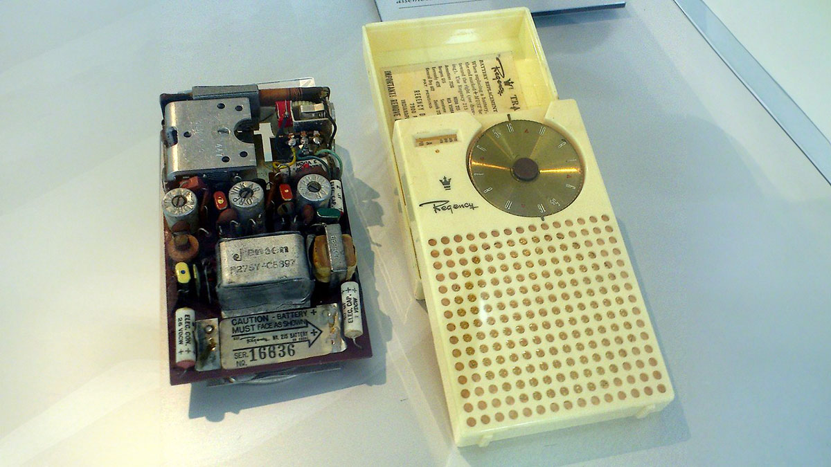 The ZX921 DIY kit I've put together is closer to the original design of the Regency TR-1 than to the final commercially available version.  The ZX921 DIY kit I've put together is closer to the original design of the Regency TR-1 than to the final commercially available version.  In addition to a push-pull, two-transformer audio amplifier, a BG4 transistor is used here as a detector instead of a diode. This is exactly what was done in the first laboratory prototype of the Regency TR-1. With superior transistors having repeatable and stable characteristics, today's new radio receiver uses a reasonable intermediate frequency of 455 kHz. Neutrodyne circuits with hand-picked capacitors are no longer needed. And to power the receiver, there's no need for 22.5, 9, or even 3 volts; 1.5 volts is enough—just one 1.5 volt battery! The diagram shows breakpoints for measuring the operating currents of transistors in the absence of an input signal. In the last century, when setting up a receiver, base bias resistors were selected for each specific transistor so that the actual currents were within the list values. Today, transistors and resistors are manufactured with much greater precision, so this setup step is completely optional. The receiver kit even comes with pre-configured heterodyne and filter coils. So, it is fine to use the signal from a nearby powerful radio station or a micro-power radio transmitter to make fine adjustments for maximum volume and sound frequency. 69 years have passed, and transistor AM superheterodynes have zero to no changes. Assembling and configuring them has become much easier but no less interesting. Even more exciting are the experiments with RF-tuned receivers, which I will talk about in the next post. |
| json metadata | {"tags":["diy"],"image":["https://cdn.steemitimages.com/DQmeooGgWCAaeYNag7XLMqggXx2UAKUMjuUQV6tLBM2b4KN/image.png","https://cdn.steemitimages.com/DQmTgeUGA46qGQSLDeR2e7y18xtDrJbZ5njwheFPAvNPiyd/image.png","https://cdn.steemitimages.com/DQmUhGALf1Xfm5fNRvjV231wkX5ZrBkd2xL2uDv2wgebSRa/image.png","https://cdn.steemitimages.com/DQmTJwjv39cVKHax7yYCaCZmoREePcY9HZJha1AaEcNQEHQ/image.png","https://cdn.steemitimages.com/DQmWPdqmKakY5hWViikeosR3Z5TJmY8ffnvimqrHuZQRwRN/image.png","https://cdn.steemitimages.com/DQmXBfKLQcvtka9HUWZ79sJbM4aaWqZiJxVUHzaV9fUgt3y/image.png","https://cdn.steemitimages.com/DQmdBGwK6J3gYUquTnrzswEULk1Ef49GFGb39Z1RHzY7GQz/image.png","https://assets-global.website-files.com/6438c93ff266bb9903cab3bc/65a7a72f8074d775f09249cc_7.jpg","https://assets-global.website-files.com/6438c93ff266bb9903cab3bc/65a7a734380ad54973117c75_8.jpg","https://assets-global.website-files.com/6438c93ff266bb9903cab3bc/65a7a73941cfc072e47fb575_9.jpg","https://cdn.steemitimages.com/DQmcFpELqxcvU99DBgTBobssqitj3ePHduRgVAzUA8LZoqh/image.png","https://assets-global.website-files.com/6438c93ff266bb9903cab3bc/65a7a747cd3d2c9585b2c08c_11.jpg","https://assets-global.website-files.com/6438c93ff266bb9903cab3bc/65a7a74ed563c9786d84d3a5_12.jpg","https://assets-global.website-files.com/6438c93ff266bb9903cab3bc/65a7a791db5d176225af3035_13.jpg","https://assets-global.website-files.com/6438c93ff266bb9903cab3bc/65a7a799eaa41b41cfd1e58d_14.jpg","https://cdn.steemitimages.com/DQmV7H8vB6tSLYuBRmbWFwtR32EnJ4PaAzmfrbtmuy1232A/image.png","https://cdn.steemitimages.com/DQmXH4kigcEzzVskYbhZUVqqitPf4ZAe6WL3GqfydahDoHZ/image.png","https://cdn.steemitimages.com/DQmVWoejYyDGg1pyk9MFhNeWUvxsHRWimBfAnNyj8ouQcwd/image.png","https://cdn.steemitimages.com/DQmdTAFr5PH12qVN7yHjAU4jN14Nh2UnYtkMiAzGyfkWL4D/image.png"],"app":"steemit/0.2","format":"markdown"} |
| parent author | |
| parent permlink | diy |
| permlink | regency-tr-1-superheterodyne-transistor-radio |
| title | Regency TR-1 superheterodyne transistor radio |
| Transaction Info | Block #81869501/Trx 66435aeeb8e02c2fd5c0ab28aabaf8b134458086 |
View Raw JSON Data
{
"block": 81869501,
"op": [
"comment",
{
"author": "teardownit",
"body": "I almost built a 1954 Regency TR-1 superheterodyne transistor radio.\n\n\n\nIt was the very first commercially available radio receiver in the United States and globally, built entirely on transistors. How much have inner and outer designs changed in 69 (excellent) years?\n\nThe 1954 Regency TR-1 was not just portable but pocket-sized. And not just pocket-sized but autonomous and battery-efficient.\n\n\n\nPocket crystal radios, such as the popular back-in-the-day rocket-shaped ones, have been around for a long time. They required grounding, so listening to the radio while walking was impossible.\n\n\n\nThe earbud cable performed the antenna function as somewhat recent cell phones with FM receiver functions. And the decorative antenna at the top of the rocket was a tuning plunger for moving the induction coil of the resonant tank core.\n\n\n\nThere were pocket tube radios in the 1950s. But an expensive set of anode and incandescent batteries lasts for just 5 hours. And almost all such receivers could only be listened to with an earbud.\n\nThere were a few loudspeaker exceptions, like a 1954 Hoffman Nugget sub-mini tube pocket radio made in Los Angeles, California.\n\n\n\nTwo marks on the receiver scale in the form of a triangle indicate 640 and 1240 kHz, the frequencies for the public warning system. In the 1950s, it became clear how important small, self-powered radios were in an emergency. This spurred demand for such receivers.\n\n\n\nAnd this is a loud-speaking 1953 Emerson 747. It was too quiet, so in 1955, the low-frequency tube output stage was replaced with a transistor one. The new model received the number 838.\n\n\n\nThe Emerson 838 was called the world's first transistor radio in ads. However, it was a hybrid tube transistor and the all-transistor Regency TR-1 had already been released a year earlier.\n\nhttps://assets-global.website-files.com/6438c93ff266bb9903cab3bc/65a7a72f8074d775f09249cc_7.jpg\n\nIt was a revolution, both technically and aesthetically. The Regency TR-1's case set the standard for radio design for decades, and no doubt even influenced the appearance of the Apple iPod.\n\nhttps://assets-global.website-files.com/6438c93ff266bb9903cab3bc/65a7a734380ad54973117c75_8.jpg\n\nNote that a thumbwheel instead of a knob was first used not in transistor receivers for the sake of compactness but in old RF-tuned radios for a completely different purpose.\n\nhttps://assets-global.website-files.com/6438c93ff266bb9903cab3bc/65a7a73941cfc072e47fb575_9.jpg\n\nFor loud-speaking reception of a signal from a powerful station, it is enough to connect an audio amplifier to the crystal radio output. And to hear a distant station, one needs to amplify a weak signal using a radio frequency amplifier.\n\nThe problem here is that the strong signal of a nearby station will not vanish into the blue. One or even two LC-resonant tanks will not be enough to suppress unwanted signals and highlight the desired ones. Therefore, a nearby station (and also interference from car ignition and other electric motors nearby) will sound louder than a distant one.\n\n\n\nRF-tuned receivers were created with three, four, and even five resonant tanks, like the 1927 Leutz Transoceanic \"Phantom\" to mitigate this issue.\n\nLinking the shafts of three or five variable RF-tuned radio capacitors mechanically and settling for just one tuning knob is, at first glance, a bad idea because it is difficult to ensure stable equality of the resonant frequencies of all resonant tanks in each position of this knob.\n\nTherefore, the creators of such receivers supplemented each variable capacitor with a dedicated adjustment regulator. Unlike the knob, which is supposed to be turned with a two-finger pinch, the thumbwheel can be rotated with one finger. Thus, one can learn to adjust three or even four circuits simultaneously.\n\nIt would be even better to make one large knob with a vernier, a reduction gear with a scale that turns the shafts of all variable capacitors, and connect an additional small variable capacitor in parallel to each big one for fine-tuning. But this would lead to a cost increase for the receiver as well as an increase in weight and dimensions.\n\nBut one can choose another path. When we tune a guitar by holding the second string at the fifth fret and listening to its sound simultaneously with the first string, we hear the vibrations with a frequency equal to the difference in frequencies of the two strings.\n\nIf we need a natural Pythagorean scale, we ensure these vibrations disappear, and the strings sound at exactly the same frequency. And if a tempered scale is required, we leave a certain number of vibrations per minute.\n\nPiano tuners know and use this, but guitarists often tune the instrument with string harmonics rather than frets. This makes it more accurate and makes it sound better. Or by an electronic tuner, which considers temperament and even adjusts the additional tension of the string when it is clamped on the fret.\n\nThe same thing happens with electrical oscillations: when oscillations of two different frequencies are mixed, the resulting oscillations occur with frequencies equal to the sum and difference of the original ones.\n\nWhat if one mixes a radio signal with the oscillations of a special local oscillator—a heterodyne—and then extracts a certain intermediate frequency from the mixture?\n\nhttps://assets-global.website-files.com/6438c93ff266bb9903cab3bc/65a7a747cd3d2c9585b2c08c_11.jpg\n\nIn this case, one can have as many intermediate frequency amplification stages as one likes with bandpass filters tuned to them, and these filters do not need to be rebuilt; they only need to be configured once when setting up the radio receiver.\n\nTo tune in to the wave of the desired station, one only needs to reconfigure the input circuit and the heterodyne circuit using dual variable capacitors. This advanced radio receiver is called a superheterodyne and has been the most common type of receiver for decades.\n\nhttps://assets-global.website-files.com/6438c93ff266bb9903cab3bc/65a7a74ed563c9786d84d3a5_12.jpg\nAnd this is what these structural blocks looked like in the real working circuit of the 1954 Regency TR-1. On the first transistor, counting from the left, a frequency converter is assembled, combining the functions of a local oscillator and a mixer.\n\nhttps://assets-global.website-files.com/6438c93ff266bb9903cab3bc/65a7a791db5d176225af3035_13.jpg\n\nThe heterodyne here is an Armstrong generator, which is not surprising: the inventor of the superheterodyne radio receiver is Edwin Howard Armstrong.\n\nAfter the heterodyne, two intermediate-frequency amplification stages with three resonant tanks are included, forming an IF filter. The two RC circuits at the top of the diagram are neutrodyne circuits that neutralize the Miller effect.\nhttps://assets-global.website-files.com/6438c93ff266bb9903cab3bc/65a7a799eaa41b41cfd1e58d_14.jpg\n\nThe transistors used in the Regency TR-1 were expensive and far from perfect. It was necessary to manually pick transistors with suitable parameters from a batch and manually select the capacitance of the neutrodyne capacitor within 100–200 pF (at the time, the correct term was uuF). We also had to use a 22.5-volt battery for power and use a low intermediate frequency of 262 kHz.\n\n\n\nThe voltage from the detector not only goes to the audio frequency amplifier but also regulates the transistor's bias in the amplifier's first IF stage. A weak signal is amplified more than an already strong one, which allows one to listen to distant and nearby stations without manually adjusting the gain. This is called automatic gain control, or AGC.\n\n\n\nInitially, the creators of the Regency TR-1 wanted to use a louder and higher-quality audio amplifier, like the Emerson 838. Still, they had to make it with a single transistor to keep the cost lower. So, despite using an excellent Jensen loudspeaker (the company creates loudspeakers for Fender amplifiers), the TR-1's sound leaves much to be desired.\n\n\n\nThe ZX921 DIY kit I've put together is closer to the original design of the Regency TR-1 than to the final commercially available version.\n\n\n\nThe ZX921 DIY kit I've put together is closer to the original design of the Regency TR-1 than to the final commercially available version.\n\n\n\nIn addition to a push-pull, two-transformer audio amplifier, a BG4 transistor is used here as a detector instead of a diode. This is exactly what was done in the first laboratory prototype of the Regency TR-1.\n\nWith superior transistors having repeatable and stable characteristics, today's new radio receiver uses a reasonable intermediate frequency of 455 kHz. Neutrodyne circuits with hand-picked capacitors are no longer needed.\n\nAnd to power the receiver, there's no need for 22.5, 9, or even 3 volts; 1.5 volts is enough—just one 1.5 volt battery!\n\nThe diagram shows breakpoints for measuring the operating currents of transistors in the absence of an input signal. In the last century, when setting up a receiver, base bias resistors were selected for each specific transistor so that the actual currents were within the list values.\n\nToday, transistors and resistors are manufactured with much greater precision, so this setup step is completely optional.\n\nThe receiver kit even comes with pre-configured heterodyne and filter coils. So, it is fine to use the signal from a nearby powerful radio station or a micro-power radio transmitter to make fine adjustments for maximum volume and sound frequency.\n\n69 years have passed, and transistor AM superheterodynes have zero to no changes. Assembling and configuring them has become much easier but no less interesting.\n\nEven more exciting are the experiments with RF-tuned receivers, which I will talk about in the next post.",
"json_metadata": "{\"tags\":[\"diy\"],\"image\":[\"https://cdn.steemitimages.com/DQmeooGgWCAaeYNag7XLMqggXx2UAKUMjuUQV6tLBM2b4KN/image.png\",\"https://cdn.steemitimages.com/DQmTgeUGA46qGQSLDeR2e7y18xtDrJbZ5njwheFPAvNPiyd/image.png\",\"https://cdn.steemitimages.com/DQmUhGALf1Xfm5fNRvjV231wkX5ZrBkd2xL2uDv2wgebSRa/image.png\",\"https://cdn.steemitimages.com/DQmTJwjv39cVKHax7yYCaCZmoREePcY9HZJha1AaEcNQEHQ/image.png\",\"https://cdn.steemitimages.com/DQmWPdqmKakY5hWViikeosR3Z5TJmY8ffnvimqrHuZQRwRN/image.png\",\"https://cdn.steemitimages.com/DQmXBfKLQcvtka9HUWZ79sJbM4aaWqZiJxVUHzaV9fUgt3y/image.png\",\"https://cdn.steemitimages.com/DQmdBGwK6J3gYUquTnrzswEULk1Ef49GFGb39Z1RHzY7GQz/image.png\",\"https://assets-global.website-files.com/6438c93ff266bb9903cab3bc/65a7a72f8074d775f09249cc_7.jpg\",\"https://assets-global.website-files.com/6438c93ff266bb9903cab3bc/65a7a734380ad54973117c75_8.jpg\",\"https://assets-global.website-files.com/6438c93ff266bb9903cab3bc/65a7a73941cfc072e47fb575_9.jpg\",\"https://cdn.steemitimages.com/DQmcFpELqxcvU99DBgTBobssqitj3ePHduRgVAzUA8LZoqh/image.png\",\"https://assets-global.website-files.com/6438c93ff266bb9903cab3bc/65a7a747cd3d2c9585b2c08c_11.jpg\",\"https://assets-global.website-files.com/6438c93ff266bb9903cab3bc/65a7a74ed563c9786d84d3a5_12.jpg\",\"https://assets-global.website-files.com/6438c93ff266bb9903cab3bc/65a7a791db5d176225af3035_13.jpg\",\"https://assets-global.website-files.com/6438c93ff266bb9903cab3bc/65a7a799eaa41b41cfd1e58d_14.jpg\",\"https://cdn.steemitimages.com/DQmV7H8vB6tSLYuBRmbWFwtR32EnJ4PaAzmfrbtmuy1232A/image.png\",\"https://cdn.steemitimages.com/DQmXH4kigcEzzVskYbhZUVqqitPf4ZAe6WL3GqfydahDoHZ/image.png\",\"https://cdn.steemitimages.com/DQmVWoejYyDGg1pyk9MFhNeWUvxsHRWimBfAnNyj8ouQcwd/image.png\",\"https://cdn.steemitimages.com/DQmdTAFr5PH12qVN7yHjAU4jN14Nh2UnYtkMiAzGyfkWL4D/image.png\"],\"app\":\"steemit/0.2\",\"format\":\"markdown\"}",
"parent_author": "",
"parent_permlink": "diy",
"permlink": "regency-tr-1-superheterodyne-transistor-radio",
"title": "Regency TR-1 superheterodyne transistor radio"
}
],
"op_in_trx": 0,
"timestamp": "2024-01-23T07:54:03",
"trx_id": "66435aeeb8e02c2fd5c0ab28aabaf8b134458086",
"trx_in_block": 0,
"virtual_op": 0
}projectdignityupvoted (100.00%) @teardownit / when-is-the-best-case-for-hdmi-over-ip-extenders2024/01/16 07:49:36
projectdignityupvoted (100.00%) @teardownit / when-is-the-best-case-for-hdmi-over-ip-extenders
2024/01/16 07:49:36
| author | teardownit |
| permlink | when-is-the-best-case-for-hdmi-over-ip-extenders |
| voter | projectdignity |
| weight | 10000 (100.00%) |
| Transaction Info | Block #81668513/Trx 6a0bb69f444b3af885894854ceb31be5b88993bc |
View Raw JSON Data
{
  "block": 81668513,
  "op": [
    "vote",
    {
      "author": "teardownit",
      "permlink": "when-is-the-best-case-for-hdmi-over-ip-extenders",
      "voter": "projectdignity",
      "weight": 10000
    }
  ],
  "op_in_trx": 0,
  "timestamp": "2024-01-16T07:49:36",
  "trx_id": "6a0bb69f444b3af885894854ceb31be5b88993bc",
  "trx_in_block": 1,
  "virtual_op": 0
}teardownitpublished a new post: when-is-the-best-case-for-hdmi-over-ip-extenders2024/01/16 07:44:42
teardownitpublished a new post: when-is-the-best-case-for-hdmi-over-ip-extenders
2024/01/16 07:44:42
| author | teardownit |
| body | IntroductionWhy use HDMI over IP in some cases? The image quality is noticeably worse than a classic HDMI twisted-pair extender. Let's see a few examples and answer this together. When is the best case for HDMI over IP extenders? Previously, we have repeatedly compared two types of HDMI extenders with each other: - HDMI over twisted pair cable - HDMI over IP extender https://assets-global.website-files.com/6438c93ff266bb9903cab3bc/659b7af2094eaac10eacb3cf_2.jpg The second type also works over twisted pairs, but it has the additional ability to operate in populated local networks. Upon reading our posts, you may think using the first type of extender is always better. After all, it is indeed better in many respects: ideal video quality, no transmission delays, and many supplemental functions. The only thing is to stay within the twisted pair cable length limits, usually up to 330 feet. But it is only sometimes the case. Sometimes, having a separate twisted-pair cable from the video source to the TV makes it impossible to install a transmitter and receiver of the first type. But suppose there are available wired Ethernet sockets somewhere near both installation spots. In that case, the extender of the second type is a good option. Sometimes, installers plan on remaking an existing LAN, adding separate twisted-pair cables for video transmission of the first type, and turning to us for advice. The initial idea is to disconnect two sections of twisted-pair cable from the router: from the video source to the router from the TV to the routerand connect both lines together. At first glance, we will see a twisted-pair cable from the video source to the TV. So we should be able to use type 1 extenders, right? Although it is theoretically possible, the probability is extremely low. We will have the following connection between the transmitter and receiver: HDMI transmitter - patch cable - LAN socket - twisted-pair cable - connector - twisted-pair cable - LAN socket - patch cable - receiver. https://assets-global.website-files.com/6438c93ff266bb9903cab3bc/659b7ba11b3593da28c3b7a3_3.jpg The first type of extender is very picky about the cable's construction and the connections between the transmitter and the receiver. Firstly, one must use twisted-pair cable of a category no lower than specified in the manual. This is usually CAT6, CAT6A, or better. Secondly, there must be a solid piece of twisted-pair cable between the HDMI transmitter and receiver with no breaks or lower-quality connectors, like wall sockets. The second type of extender works like any other LAN device. So, we can use LAN sockets, patch cords, routers, and switches. Of course, expensive professional solutions with low video compression levels exist. The quality of the video output from the receiver is hard to distinguish from the original. The transmission delay is almost invisible to the human eye. Such equipment has strict requirements from the manufacturers in terms of IP-network parameters; they usually do not recommend using an existing network. In our post, we will skip this case and look at more down-to-earth options for the average user. So what are you going to do if laying a separate whole piece of twisted pair is not on the options list? First, you must determine what you will connect to the remote TV. Suppose this is a DVR located somewhere in the attic or garage. In that case, you can safely use an HDMI over IP extender connected to the existing LAN network. Let's look at one of the devices of this sort and try it in real-world conditions. We'll use the INRIKS EX2073KVM extender as an example. >Device description https://assets-global.website-files.com/6438c93ff266bb9903cab3bc/659b7baa6a43dcf0de6242b6_4.jpg The INRIKS EX2073KVM is an HDMI and USB transmitter and receiver kit twisted-pair cable with a range of up to 390 feet. The kit operates "over IP," so the receiver can be connected to the transmitter with a single piece of twisted pair and via a local network. The maximum video resolution is 1080p at 60 Hz. In addition to video, the EX2073KVM can transmit a USB 1.1 signal, which is sufficient for a USB keyboard and a USB mouse. Let's look closer at the package contents and the typical connection. >Visual overview As usual, the HDMI over twisted pair extender INRIKS EX2073KVM is shipped in a standard gray box. The sticker lists the main parameters that the kit provides. https://assets-global.website-files.com/6438c93ff266bb9903cab3bc/659b7bb3fccf5c14ab541a50_5.jpg Having opened the box, we immediately see the transmitter and receiver in a separate tray. https://assets-global.website-files.com/6438c93ff266bb9903cab3bc/659b7bba36da2c69fdbdcfca_6.jpg The remaining components of the kit are located under it. https://assets-global.website-files.com/6438c93ff266bb9903cab3bc/659b7bc3ed3a128a9123fd32_7.jpg So, the INRIKS EX2073KVM kit consists of: Transmitter unit - 1 pc Receiver unit - 1 pc DC 5V/1A - 2 pcs USB Cable - 1 pc User manual - 1 pc The transmitter and receiver are of average size and feel substantial in the hand due to the case metal thickness. https://assets-global.website-files.com/6438c93ff266bb9903cab3bc/659b7bd7e94344098dd1f9e9_8.jpg https://assets-global.website-files.com/6438c93ff266bb9903cab3bc/659b7bdc62a8f0dafa3d86f9_9.jpg https://assets-global.website-files.com/6438c93ff266bb9903cab3bc/659b7be15c622aebe36f1f94_10.jpg https://assets-global.website-files.com/6438c93ff266bb9903cab3bc/659b7be5faadfb8ed921fe9f_11.jpg The transmitter has the following connectors: - DC 5V power input - HDMI IN for connecting a video source (PC or DVR) - USB PC for connecting to a video source for remote control - 3×LED indicators - LAN TX for twisted pair connection - Reset button The receiver has the following connectors: - DC 5V power input - HDMI OUT for connecting a TV - 2×USB for connecting the keyboard and mouse - 3×LED indicators - LAN RX for twisted pair connection - Reset button As you may have already noticed, the kit has minimal connectors for transmitting HDMI and USB keyboard/mouse interfaces over twisted-pair cables. This is true and emphasizes the device's one and only function. Unlike many other INRIKS extenders, our kit has neither fixed nor detachable surface mounting brackets. We consider this a downside. https://assets-global.website-files.com/6438c93ff266bb9903cab3bc/659b7bf0264ad19f20bad4e3_12.jpg Having opened the top cover of the transmitter, we once again ensured that the metal that the case was made of was thick. Or rather, its upper part. https://assets-global.website-files.com/6438c93ff266bb9903cab3bc/659b7bfbac9629131744541b_13.jpg Next, we were a bit surprised. Inside, we found not one PCB, as is usually the case with such devices, but two. The boards are interconnected with a flat cable. https://assets-global.website-files.com/6438c93ff266bb9903cab3bc/659b7c0721eecb2ee0eccaa4_14.jpg The receiver also has two boards. The soldering quality is quite good. There are minor stains on certain elements. Most likely, there should be no impact on the operation. The back side of the boards is less neat. There are minor stains that are already typical for the entire line of INRIKS equipment. https://assets-global.website-files.com/6438c93ff266bb9903cab3bc/659b7c1bfa40353fbaa064e4_16.jpg Testing Initially, we decided to test the device under almost ideal conditions. Connect the transmitter and receiver with a single piece of CAT6 330-foot twisted-pair cable. We connected a laptop to the transmitter and a monitor, keyboard, and mouse to the receiver. After powering it on, everything worked within a few seconds. Because the laptop and the "remote" monitor are located nearby in our case, the eye notices a slight lag in the image on the remote monitor. This is typical for most HDMI over IP extenders. This delay is also felt when controlling the mouse, which causes slight discomfort. We conclude for ourselves that this technology is not suitable for day-to-day working on a remote PC. We measured the latency between the laptop screen and the remote monitor. It averaged 0.08 seconds. As expected, the video quality on the remote monitor suffered a little. It is very difficult to notice the deterioration while watching the video. But when displaying menus and similar static images, sometimes the moire around some letters is slightly noticeable. This is due to video compression and decompression during "over IP" transmission. The next step is to connect the transmitter and the receiver to our existing local network, according to the diagram below.  Please note that we used short patch cables to connect the transmitter and the receiver to LAN sockets. After powering on the equipment, everything worked as expected in a few seconds, and the average latency value did not change. Conclusion In this article, we decided to show another subtle advantage of using an HDMI over an IP extender. Such devices are more forgiving when it comes to cable connections. Therefore, if you manage to lay a separate twisted-pair cable of the required category, it is better to use an HDMI extender of the first type to get an excellent result. If you are going to use an existing cable that someone else installed in the wall before you, you will most likely have to use the second type of HDMI extender, an IP-based one. If you have no choice but to use an existing LAN, then the option here is obvious :) The area of application of such extenders is also critical. This option can even be called optimal if you use them for CCTV (connecting a TV and mouse remote from the DVR). |
| json metadata | {"tags":["hdmi"],"image":["https://assets-global.website-files.com/6438c93ff266bb9903cab3bc/659b7af2094eaac10eacb3cf_2.jpg","https://assets-global.website-files.com/6438c93ff266bb9903cab3bc/659b7ba11b3593da28c3b7a3_3.jpg","https://assets-global.website-files.com/6438c93ff266bb9903cab3bc/659b7baa6a43dcf0de6242b6_4.jpg","https://assets-global.website-files.com/6438c93ff266bb9903cab3bc/659b7bb3fccf5c14ab541a50_5.jpg","https://assets-global.website-files.com/6438c93ff266bb9903cab3bc/659b7bba36da2c69fdbdcfca_6.jpg","https://assets-global.website-files.com/6438c93ff266bb9903cab3bc/659b7bc3ed3a128a9123fd32_7.jpg","https://assets-global.website-files.com/6438c93ff266bb9903cab3bc/659b7bd7e94344098dd1f9e9_8.jpg","https://assets-global.website-files.com/6438c93ff266bb9903cab3bc/659b7bdc62a8f0dafa3d86f9_9.jpg","https://assets-global.website-files.com/6438c93ff266bb9903cab3bc/659b7be15c622aebe36f1f94_10.jpg","https://assets-global.website-files.com/6438c93ff266bb9903cab3bc/659b7be5faadfb8ed921fe9f_11.jpg","https://assets-global.website-files.com/6438c93ff266bb9903cab3bc/659b7bf0264ad19f20bad4e3_12.jpg","https://assets-global.website-files.com/6438c93ff266bb9903cab3bc/659b7bfbac9629131744541b_13.jpg","https://assets-global.website-files.com/6438c93ff266bb9903cab3bc/659b7c0721eecb2ee0eccaa4_14.jpg","https://assets-global.website-files.com/6438c93ff266bb9903cab3bc/659b7c1bfa40353fbaa064e4_16.jpg","https://cdn.steemitimages.com/DQmSeZkQfrrUqjhePAuvqX7yVA7u4o5UuQ379FfDHRVVPgC/image.png"],"app":"steemit/0.2","format":"markdown"} |
| parent author | |
| parent permlink | hdmi |
| permlink | when-is-the-best-case-for-hdmi-over-ip-extenders |
| title | When is the best case for HDMI over IP extenders? |
| Transaction Info | Block #81668415/Trx c194e7782b0d99768161497e63b51d443c626200 |
View Raw JSON Data
{
"block": 81668415,
"op": [
"comment",
{
"author": "teardownit",
"body": "IntroductionWhy use HDMI over IP in some cases? The image quality is noticeably worse than a classic HDMI twisted-pair extender. Let's see a few examples and answer this together.\n\nWhen is the best case for HDMI over IP extenders?\n\nPreviously, we have repeatedly compared two types of HDMI extenders with each other:\n\n- HDMI over twisted pair cable\n- HDMI over IP extender\n\nhttps://assets-global.website-files.com/6438c93ff266bb9903cab3bc/659b7af2094eaac10eacb3cf_2.jpg\nThe second type also works over twisted pairs, but it has the additional ability to operate in populated local networks.\n\nUpon reading our posts, you may think using the first type of extender is always better. After all, it is indeed better in many respects: ideal video quality, no transmission delays, and many supplemental functions. The only thing is to stay within the twisted pair cable length limits, usually up to 330 feet.\n\nBut it is only sometimes the case.\n\nSometimes, having a separate twisted-pair cable from the video source to the TV makes it impossible to install a transmitter and receiver of the first type. But suppose there are available wired Ethernet sockets somewhere near both installation spots. In that case, the extender of the second type is a good option.\n\nSometimes, installers plan on remaking an existing LAN, adding separate twisted-pair cables for video transmission of the first type, and turning to us for advice. The initial idea is to disconnect two sections of twisted-pair cable from the router:\n\nfrom the video source to the router\nfrom the TV to the routerand connect both lines together.\nAt first glance, we will see a twisted-pair cable from the video source to the TV. So we should be able to use type 1 extenders, right? Although it is theoretically possible, the probability is extremely low.\n\nWe will have the following connection between the transmitter and receiver: HDMI transmitter - patch cable - LAN socket - twisted-pair cable - connector - twisted-pair cable - LAN socket - patch cable - receiver.\n\nhttps://assets-global.website-files.com/6438c93ff266bb9903cab3bc/659b7ba11b3593da28c3b7a3_3.jpg\n\nThe first type of extender is very picky about the cable's construction and the connections between the transmitter and the receiver. Firstly, one must use twisted-pair cable of a category no lower than specified in the manual. This is usually CAT6, CAT6A, or better. Secondly, there must be a solid piece of twisted-pair cable between the HDMI transmitter and receiver with no breaks or lower-quality connectors, like wall sockets.\n\nThe second type of extender works like any other LAN device. So, we can use LAN sockets, patch cords, routers, and switches.\n\nOf course, expensive professional solutions with low video compression levels exist. The quality of the video output from the receiver is hard to distinguish from the original. The transmission delay is almost invisible to the human eye. Such equipment has strict requirements from the manufacturers in terms of IP-network parameters; they usually do not recommend using an existing network.\n\nIn our post, we will skip this case and look at more down-to-earth options for the average user.\n\nSo what are you going to do if laying a separate whole piece of twisted pair is not on the options list? First, you must determine what you will connect to the remote TV. Suppose this is a DVR located somewhere in the attic or garage. In that case, you can safely use an HDMI over IP extender connected to the existing LAN network.\n\nLet's look at one of the devices of this sort and try it in real-world conditions. We'll use the INRIKS EX2073KVM extender as an example.\n\n>Device description\n\nhttps://assets-global.website-files.com/6438c93ff266bb9903cab3bc/659b7baa6a43dcf0de6242b6_4.jpg\n\nThe INRIKS EX2073KVM is an HDMI and USB transmitter and receiver kit twisted-pair cable with a range of up to 390 feet. The kit operates \"over IP,\" so the receiver can be connected to the transmitter with a single piece of twisted pair and via a local network.\n\nThe maximum video resolution is 1080p at 60 Hz.\n\nIn addition to video, the EX2073KVM can transmit a USB 1.1 signal, which is sufficient for a USB keyboard and a USB mouse.\n\nLet's look closer at the package contents and the typical connection.\n\n>Visual overview\n\nAs usual, the HDMI over twisted pair extender INRIKS EX2073KVM is shipped in a standard gray box. The sticker lists the main parameters that the kit provides.\n\nhttps://assets-global.website-files.com/6438c93ff266bb9903cab3bc/659b7bb3fccf5c14ab541a50_5.jpg\nHaving opened the box, we immediately see the transmitter and receiver in a separate tray.\n\nhttps://assets-global.website-files.com/6438c93ff266bb9903cab3bc/659b7bba36da2c69fdbdcfca_6.jpg\nThe remaining components of the kit are located under it.\n\nhttps://assets-global.website-files.com/6438c93ff266bb9903cab3bc/659b7bc3ed3a128a9123fd32_7.jpg\nSo, the INRIKS EX2073KVM kit consists of:\n\nTransmitter unit - 1 pc\nReceiver unit - 1 pc\nDC 5V/1A - 2 pcs\nUSB Cable - 1 pc\nUser manual - 1 pc\nThe transmitter and receiver are of average size and feel substantial in the hand due to the case metal thickness.\n\nhttps://assets-global.website-files.com/6438c93ff266bb9903cab3bc/659b7bd7e94344098dd1f9e9_8.jpg\nhttps://assets-global.website-files.com/6438c93ff266bb9903cab3bc/659b7bdc62a8f0dafa3d86f9_9.jpg\nhttps://assets-global.website-files.com/6438c93ff266bb9903cab3bc/659b7be15c622aebe36f1f94_10.jpg\nhttps://assets-global.website-files.com/6438c93ff266bb9903cab3bc/659b7be5faadfb8ed921fe9f_11.jpg\n\nThe transmitter has the following connectors:\n\n- DC 5V power input\n- HDMI IN for connecting a video source (PC or DVR)\n- USB PC for connecting to a video source for remote control\n- 3×LED indicators\n- LAN TX for twisted pair connection\n- Reset button\n\nThe receiver has the following connectors:\n\n- DC 5V power input\n- HDMI OUT for connecting a TV\n- 2×USB for connecting the keyboard and mouse\n- 3×LED indicators\n- LAN RX for twisted pair connection\n- Reset button\n\nAs you may have already noticed, the kit has minimal connectors for transmitting HDMI and USB keyboard/mouse interfaces over twisted-pair cables. This is true and emphasizes the device's one and only function.\n\nUnlike many other INRIKS extenders, our kit has neither fixed nor detachable surface mounting brackets. We consider this a downside.\n\nhttps://assets-global.website-files.com/6438c93ff266bb9903cab3bc/659b7bf0264ad19f20bad4e3_12.jpg\n\nHaving opened the top cover of the transmitter, we once again ensured that the metal that the case was made of was thick. Or rather, its upper part.\n\nhttps://assets-global.website-files.com/6438c93ff266bb9903cab3bc/659b7bfbac9629131744541b_13.jpg\n\nNext, we were a bit surprised. Inside, we found not one PCB, as is usually the case with such devices, but two. The boards are interconnected with a flat cable.\n\nhttps://assets-global.website-files.com/6438c93ff266bb9903cab3bc/659b7c0721eecb2ee0eccaa4_14.jpg\n\nThe receiver also has two boards.\nThe soldering quality is quite good. There are minor stains on certain elements. Most likely, there should be no impact on the operation.\n\nThe back side of the boards is less neat. There are minor stains that are already typical for the entire line of INRIKS equipment.\n\nhttps://assets-global.website-files.com/6438c93ff266bb9903cab3bc/659b7c1bfa40353fbaa064e4_16.jpg\n\nTesting\n\nInitially, we decided to test the device under almost ideal conditions. Connect the transmitter and receiver with a single piece of CAT6 330-foot twisted-pair cable. We connected a laptop to the transmitter and a monitor, keyboard, and mouse to the receiver.\n\nAfter powering it on, everything worked within a few seconds. Because the laptop and the \"remote\" monitor are located nearby in our case, the eye notices a slight lag in the image on the remote monitor. This is typical for most HDMI over IP extenders. This delay is also felt when controlling the mouse, which causes slight discomfort.\n\nWe conclude for ourselves that this technology is not suitable for day-to-day working on a remote PC.\n\nWe measured the latency between the laptop screen and the remote monitor. It averaged 0.08 seconds.\n\nAs expected, the video quality on the remote monitor suffered a little. It is very difficult to notice the deterioration while watching the video. But when displaying menus and similar static images, sometimes the moire around some letters is slightly noticeable. This is due to video compression and decompression during \"over IP\" transmission.\n\nThe next step is to connect the transmitter and the receiver to our existing local network, according to the diagram below.\n\n\n\nPlease note that we used short patch cables to connect the transmitter and the receiver to LAN sockets.\n\nAfter powering on the equipment, everything worked as expected in a few seconds, and the average latency value did not change.\nConclusion\nIn this article, we decided to show another subtle advantage of using an HDMI over an IP extender. Such devices are more forgiving when it comes to cable connections.\n\nTherefore, if you manage to lay a separate twisted-pair cable of the required category, it is better to use an HDMI extender of the first type to get an excellent result.\n\nIf you are going to use an existing cable that someone else installed in the wall before you, you will most likely have to use the second type of HDMI extender, an IP-based one.\n\nIf you have no choice but to use an existing LAN, then the option here is obvious :)\n\nThe area of application of such extenders is also critical. This option can even be called optimal if you use them for CCTV (connecting a TV and mouse remote from the DVR).",
"json_metadata": "{\"tags\":[\"hdmi\"],\"image\":[\"https://assets-global.website-files.com/6438c93ff266bb9903cab3bc/659b7af2094eaac10eacb3cf_2.jpg\",\"https://assets-global.website-files.com/6438c93ff266bb9903cab3bc/659b7ba11b3593da28c3b7a3_3.jpg\",\"https://assets-global.website-files.com/6438c93ff266bb9903cab3bc/659b7baa6a43dcf0de6242b6_4.jpg\",\"https://assets-global.website-files.com/6438c93ff266bb9903cab3bc/659b7bb3fccf5c14ab541a50_5.jpg\",\"https://assets-global.website-files.com/6438c93ff266bb9903cab3bc/659b7bba36da2c69fdbdcfca_6.jpg\",\"https://assets-global.website-files.com/6438c93ff266bb9903cab3bc/659b7bc3ed3a128a9123fd32_7.jpg\",\"https://assets-global.website-files.com/6438c93ff266bb9903cab3bc/659b7bd7e94344098dd1f9e9_8.jpg\",\"https://assets-global.website-files.com/6438c93ff266bb9903cab3bc/659b7bdc62a8f0dafa3d86f9_9.jpg\",\"https://assets-global.website-files.com/6438c93ff266bb9903cab3bc/659b7be15c622aebe36f1f94_10.jpg\",\"https://assets-global.website-files.com/6438c93ff266bb9903cab3bc/659b7be5faadfb8ed921fe9f_11.jpg\",\"https://assets-global.website-files.com/6438c93ff266bb9903cab3bc/659b7bf0264ad19f20bad4e3_12.jpg\",\"https://assets-global.website-files.com/6438c93ff266bb9903cab3bc/659b7bfbac9629131744541b_13.jpg\",\"https://assets-global.website-files.com/6438c93ff266bb9903cab3bc/659b7c0721eecb2ee0eccaa4_14.jpg\",\"https://assets-global.website-files.com/6438c93ff266bb9903cab3bc/659b7c1bfa40353fbaa064e4_16.jpg\",\"https://cdn.steemitimages.com/DQmSeZkQfrrUqjhePAuvqX7yVA7u4o5UuQ379FfDHRVVPgC/image.png\"],\"app\":\"steemit/0.2\",\"format\":\"markdown\"}",
"parent_author": "",
"parent_permlink": "hdmi",
"permlink": "when-is-the-best-case-for-hdmi-over-ip-extenders",
"title": "When is the best case for HDMI over IP extenders?"
}
],
"op_in_trx": 0,
"timestamp": "2024-01-16T07:44:42",
"trx_id": "c194e7782b0d99768161497e63b51d443c626200",
"trx_in_block": 0,
"virtual_op": 0
}bluesnipersent 0.010 STEEM to @teardownit- "Hello. Good to see you on Steem. To maximize your rewards, publish your post also on Hive ( hive.blog ) and Blurt ( blurt.blog ) blockchains. Use upvu, jsup or ctime and get instant upvotes"2024/01/10 07:43:45
bluesnipersent 0.010 STEEM to @teardownit- "Hello. Good to see you on Steem. To maximize your rewards, publish your post also on Hive ( hive.blog ) and Blurt ( blurt.blog ) blockchains. Use upvu, jsup or ctime and get instant upvotes"
2024/01/10 07:43:45
| amount | 0.010 STEEM |
| from | bluesniper |
| memo | Hello. Good to see you on Steem. To maximize your rewards, publish your post also on Hive ( hive.blog ) and Blurt ( blurt.blog ) blockchains. Use upvu, jsup or ctime and get instant upvotes |
| to | teardownit |
| Transaction Info | Block #81496240/Trx ab11f02342c40f351c6f4e579beb03a658b4ebd9 |
View Raw JSON Data
{
  "block": 81496240,
  "op": [
    "transfer",
    {
      "amount": "0.010 STEEM",
      "from": "bluesniper",
      "memo": "Hello. Good to see you on Steem. To maximize your rewards, publish your post also on Hive ( hive.blog ) and Blurt ( blurt.blog ) blockchains. Use upvu, jsup or ctime and get instant upvotes",
      "to": "teardownit"
    }
  ],
  "op_in_trx": 0,
  "timestamp": "2024-01-10T07:43:45",
  "trx_id": "ab11f02342c40f351c6f4e579beb03a658b4ebd9",
  "trx_in_block": 0,
  "virtual_op": 0
}2024/01/10 07:43:21
2024/01/10 07:43:21
| author | teardownit |
| permlink | reflectometers-for-metal-cables-noise-filtering-propagation-coefficient-and-its-determination-methods |
| voter | bluesniper |
| weight | 10000 (100.00%) |
| Transaction Info | Block #81496232/Trx 665f1fc09a6f739e470eefd0ae8e4ed664ec7a45 |
View Raw JSON Data
{
  "block": 81496232,
  "op": [
    "vote",
    {
      "author": "teardownit",
      "permlink": "reflectometers-for-metal-cables-noise-filtering-propagation-coefficient-and-its-determination-methods",
      "voter": "bluesniper",
      "weight": 10000
    }
  ],
  "op_in_trx": 0,
  "timestamp": "2024-01-10T07:43:21",
  "trx_id": "665f1fc09a6f739e470eefd0ae8e4ed664ec7a45",
  "trx_in_block": 4,
  "virtual_op": 0
}2024/01/10 07:38:00
2024/01/10 07:38:00
| author | teardownit |
| body | Let's see how the cables measure influence the range of the reflectometer. How do the noise filtering mode and methods for determining the unknown propagation coefficient affect the measurement accuracy? >KEY FACTORS FOR CABLES The reflectometer's detection range depends on the cross-section of the cable cores, the overall quality of the cable, as well as on the way the reflectometer is connected to the cable being tested. The larger the cross-section of the cable cores, the less attenuation the electrical pulse supplied by the reflectometer to this cable undergoes and the longer the distance it covers. Old or defective cables may have reduced insulation resistance or increased attenuation. This significantly reduces the ability of the cable cores to conduct electrical signals and, as a result, reduces the maximum distance. The connection of the reflectometer to the cable must be done so that a pulse with the maximum possible amount of energy is emitted from the reflectometer to the cable. NOISE FILTERING I want to eliminate the noise in more detail, as it is on any cable. Many reflectometers have a digital noise filtering mode that obliterates the noise from 50 Hz to 1 GHz. This mode is designed primarily for lineworkers dealing with cables near sources of strong electromagnetic interference (for example, railway contact networks, power lines, or antenna poles). The operator can select a filter type with the required characteristics for each test to ensure the acceptable quality of the resulting reflectogram. Suppose an unexpected random voltage value appears in the line during the measurement. In that case, the noise-filtering mode gets turned on automatically. A multi-level and multifunctional filtering system allows one to check antennas and cellular nodes with some received signal interference.  In some cases, the noise-filtering subsystem may slow down the OTDR operation to such an extent that the display becomes unusable. A good example is filtering the noise the power supply induces (60 Hz). One period of alternating current with a frequency of 60 Hz is 16.7 ms. Therefore, it also takes 16.7 ms to generate one point on the reflectometer display. It will take no less than 5.12 seconds to refresh all the 256 image pixels on the display. One way to compensate for this delay is to store the denoised reflectogram. Writing data to the device memory will take some time, but subsequent operations will be as fast as if the filter were turned off. The "averaging" mode, often provided by the manufacturer to eliminate interference at maximum gain, is no exception. This mode also decreases the refresh rate of the display. Four times less noise means the screen is refreshed sixteen times slower. When the image refresh speed is reduced significantly, it becomes difficult to work with the display, so this mode should be used only when necessary. One more thing to mention: cables for digital data transmission should be tested using short pulses with a duration of 2, 10, or, in extreme cases, 100 ns. They do not affect nearby pairs under load, so the data transmission devices' error detection system will not flag them as such. PROPAGATION COEFFICIENT AND METHODS FOR ITS DETERMINATION As already mentioned, the reflectometer determines the distance to the abnormal spot based on the signal propagation speed in the cable and the time it takes to reach the point in question and return. In most cases, speed is expressed as a unitless coefficient, the ratio of the signal propagation speed in a given cable to the speed of light. It is an empirically determined value. Reflectometers from different manufacturers require one to set the wave propagation speed, called the Velocity of Propagation (VOP) or Velocity Factor (VF). Typically, this parameter is expressed as a fraction of the speed of light and can have a value from 0.3 to 1. A cable with a VOP value of 0.66 allows an electrical signal to be transmitted at 66% of the speed of light. Some manufacturers express this parameter in terms of actual speed, and then it can range from 45 to 150 m/ms. The choice of the VOP (VF) parameter significantly impacts the accuracy of any measurement made. Therefore, to obtain the most correct results possible, it is necessary to learn the methods for determining the propagation factor for each specific cable. VOP DETERMINATION METHODS UNDER DIFFERENT CONDITIONS Suppose the pulse propagation coefficient for the cable is unknown. In that case, an experiment can either calculate or determine it. 1. The insulating material's dielectric constant (ε) is a known value. VOP=1/√(ε), where ε is the relative dielectric constant for a given cable. For example, for polyethylene, ε = 2.25. Therefore, VOP = 1/√2.25 = 0.667. 2. For the first experiment, one needs a short cable of the same type as the tested cable. Connect the reflectometer to the cable section and adjust it so that the pulse reflected from the end of the section is clearly visible on the display. Move the cursor to the beginning of the pulse and start changing the VOP coefficient until the measured distance to the end of the cable is equal to its actual length (mind the length of the leads). The longer the cable, the more accurate the obtained VOP value will be. 3. A similar experiment occurs when the cable length is known, and it has a non-defective pair. Connect the reflectometer to the pair and adjust VOP until you get the cable length you already know on the screen. Again, account for the probing leads. Suppose this technique is applied to thick multi-pair cables. In that case, ensuring that the reference and tested pairs belong to the same cable layer is necessary. The length of a pair of outer layers significantly exceeds the length of a pair of inner ones. 4. If the cable length is known, but there is no suitable pair for comparison, then it is necessary to have access to the cable from both sides. https://assets-global.website-files.com/6438c93ff266bb9903cab3bc/65952e7f45fc572c482fe18e_2.jpg Roughly pick a VOP value and determine the approximate distance (L1) to the fault on side A. Using the same VOP value, determine the approximate distance (L2) to the fault on side B. The exact distance to the damage can be calculated with L1 and L2. From side A, according to the formula: (L1/(L1 + L2)) x L, where L is the known cable length. From side B, according to the formula: (L2/(L1 + L2)) x L, where L is the known cable length. |
| json metadata | {"tags":["tdr"],"image":["https://cdn.steemitimages.com/DQmXZStRiHFgUJP9LxiNsYtrJRZAyLg7v54HBGBvZ2TnoYK/image.png","https://assets-global.website-files.com/6438c93ff266bb9903cab3bc/65952e7f45fc572c482fe18e_2.jpg"],"app":"steemit/0.2","format":"markdown"} |
| parent author | |
| parent permlink | tdr |
| permlink | reflectometers-for-metal-cables-noise-filtering-propagation-coefficient-and-its-determination-methods |
| title | Reflectometers for metal cables: noise filtering, propagation coefficient, and its determination methods |
| Transaction Info | Block #81496125/Trx ba983d30cc534e8a1787e86dee6418daab1054a7 |
View Raw JSON Data
{
"block": 81496125,
"op": [
"comment",
{
"author": "teardownit",
"body": "Let's see how the cables measure influence the range of the reflectometer. How do the noise filtering mode and methods for determining the unknown propagation coefficient affect the measurement accuracy?\n\n>KEY FACTORS FOR CABLES\n\nThe reflectometer's detection range depends on the cross-section of the cable cores, the overall quality of the cable, as well as on the way the reflectometer is connected to the cable being tested.\nThe larger the cross-section of the cable cores, the less attenuation the electrical pulse supplied by the reflectometer to this cable undergoes and the longer the distance it covers.\nOld or defective cables may have reduced insulation resistance or increased attenuation. This significantly reduces the ability of the cable cores to conduct electrical signals and, as a result, reduces the maximum distance.\nThe connection of the reflectometer to the cable must be done so that a pulse with the maximum possible amount of energy is emitted from the reflectometer to the cable.\n\nNOISE FILTERING\nI want to eliminate the noise in more detail, as it is on any cable. Many reflectometers have a digital noise filtering mode that obliterates the noise from 50 Hz to 1 GHz. This mode is designed primarily for lineworkers dealing with cables near sources of strong electromagnetic interference (for example, railway contact networks, power lines, or antenna poles). The operator can select a filter type with the required characteristics for each test to ensure the acceptable quality of the resulting reflectogram.\nSuppose an unexpected random voltage value appears in the line during the measurement. In that case, the noise-filtering mode gets turned on automatically.\nA multi-level and multifunctional filtering system allows one to check antennas and cellular nodes with some received signal interference.\n\n\n\n\nIn some cases, the noise-filtering subsystem may slow down the OTDR operation to such an extent that the display becomes unusable. A good example is filtering the noise the power supply induces (60 Hz). One period of alternating current with a frequency of 60 Hz is 16.7 ms. Therefore, it also takes 16.7 ms to generate one point on the reflectometer display. It will take no less than 5.12 seconds to refresh all the 256 image pixels on the display. One way to compensate for this delay is to store the denoised reflectogram. Writing data to the device memory will take some time, but subsequent operations will be as fast as if the filter were turned off.\nThe \"averaging\" mode, often provided by the manufacturer to eliminate interference at maximum gain, is no exception. This mode also decreases the refresh rate of the display. Four times less noise means the screen is refreshed sixteen times slower. When the image refresh speed is reduced significantly, it becomes difficult to work with the display, so this mode should be used only when necessary.\nOne more thing to mention: cables for digital data transmission should be tested using short pulses with a duration of 2, 10, or, in extreme cases, 100 ns. They do not affect nearby pairs under load, so the data transmission devices' error detection system will not flag them as such.\n\nPROPAGATION COEFFICIENT AND METHODS FOR ITS DETERMINATION\nAs already mentioned, the reflectometer determines the distance to the abnormal spot based on the signal propagation speed in the cable and the time it takes to reach the point in question and return. In most cases, speed is expressed as a unitless coefficient, the ratio of the signal propagation speed in a given cable to the speed of light. It is an empirically determined value. Reflectometers from different manufacturers require one to set the wave propagation speed, called the Velocity of Propagation (VOP) or Velocity Factor (VF). Typically, this parameter is expressed as a fraction of the speed of light and can have a value from 0.3 to 1. A cable with a VOP value of 0.66 allows an electrical signal to be transmitted at 66% of the speed of light. Some manufacturers express this parameter in terms of actual speed, and then it can range from 45 to 150 m/ms.\nThe choice of the VOP (VF) parameter significantly impacts the accuracy of any measurement made. Therefore, to obtain the most correct results possible, it is necessary to learn the methods for determining the propagation factor for each specific cable.\n\nVOP DETERMINATION METHODS UNDER DIFFERENT CONDITIONS\nSuppose the pulse propagation coefficient for the cable is unknown. In that case, an experiment can either calculate or determine it.\n\n1. The insulating material's dielectric constant (ε) is a known value.\n\nVOP=1/√(ε),\n\nwhere ε is the relative dielectric constant for a given cable. For example, for polyethylene, ε = 2.25. Therefore, VOP = 1/√2.25 = 0.667.\n\n2. For the first experiment, one needs a short cable of the same type as the tested cable.\nConnect the reflectometer to the cable section and adjust it so that the pulse reflected from the end of the section is clearly visible on the display. Move the cursor to the beginning of the pulse and start changing the VOP coefficient until the measured distance to the end of the cable is equal to its actual length (mind the length of the leads).\nThe longer the cable, the more accurate the obtained VOP value will be.\n\n3. A similar experiment occurs when the cable length is known, and it has a non-defective pair.\nConnect the reflectometer to the pair and adjust VOP until you get the cable length you already know on the screen. Again, account for the probing leads.\nSuppose this technique is applied to thick multi-pair cables. In that case, ensuring that the reference and tested pairs belong to the same cable layer is necessary. The length of a pair of outer layers significantly exceeds the length of a pair of inner ones.\n\n4. If the cable length is known, but there is no suitable pair for comparison, then it is necessary to have access to the cable from both sides.\n\nhttps://assets-global.website-files.com/6438c93ff266bb9903cab3bc/65952e7f45fc572c482fe18e_2.jpg\n\nRoughly pick a VOP value and determine the approximate distance (L1) to the fault on side A. Using the same VOP value, determine the approximate distance (L2) to the fault on side B.\nThe exact distance to the damage can be calculated with L1 and L2.\n\nFrom side A, according to the formula:\n(L1/(L1 + L2)) x L, where L is the known cable length.\nFrom side B, according to the formula:\n(L2/(L1 + L2)) x L, where L is the known cable length.",
"json_metadata": "{\"tags\":[\"tdr\"],\"image\":[\"https://cdn.steemitimages.com/DQmXZStRiHFgUJP9LxiNsYtrJRZAyLg7v54HBGBvZ2TnoYK/image.png\",\"https://assets-global.website-files.com/6438c93ff266bb9903cab3bc/65952e7f45fc572c482fe18e_2.jpg\"],\"app\":\"steemit/0.2\",\"format\":\"markdown\"}",
"parent_author": "",
"parent_permlink": "tdr",
"permlink": "reflectometers-for-metal-cables-noise-filtering-propagation-coefficient-and-its-determination-methods",
"title": "Reflectometers for metal cables: noise filtering, propagation coefficient, and its determination methods"
}
],
"op_in_trx": 0,
"timestamp": "2024-01-10T07:38:00",
"trx_id": "ba983d30cc534e8a1787e86dee6418daab1054a7",
"trx_in_block": 0,
"virtual_op": 0
}bluesnipersent 0.010 STEEM to @teardownit- "Hello. Good to see you on Steem. To maximize your rewards, publish your post also on Hive ( hive.blog ) and Blurt ( blurt.blog ) blockchains. Use upvu, jsup or ctime and get instant upvotes"2024/01/03 07:54:15
bluesnipersent 0.010 STEEM to @teardownit- "Hello. Good to see you on Steem. To maximize your rewards, publish your post also on Hive ( hive.blog ) and Blurt ( blurt.blog ) blockchains. Use upvu, jsup or ctime and get instant upvotes"
2024/01/03 07:54:15
| amount | 0.010 STEEM |
| from | bluesniper |
| memo | Hello. Good to see you on Steem. To maximize your rewards, publish your post also on Hive ( hive.blog ) and Blurt ( blurt.blog ) blockchains. Use upvu, jsup or ctime and get instant upvotes |
| to | teardownit |
| Transaction Info | Block #81295531/Trx dbc36647ae91fee33cbdbf98836c676131e65cf0 |
View Raw JSON Data
{
  "block": 81295531,
  "op": [
    "transfer",
    {
      "amount": "0.010 STEEM",
      "from": "bluesniper",
      "memo": "Hello. Good to see you on Steem. To maximize your rewards, publish your post also on Hive ( hive.blog ) and Blurt ( blurt.blog ) blockchains. Use upvu, jsup or ctime and get instant upvotes",
      "to": "teardownit"
    }
  ],
  "op_in_trx": 0,
  "timestamp": "2024-01-03T07:54:15",
  "trx_id": "dbc36647ae91fee33cbdbf98836c676131e65cf0",
  "trx_in_block": 2,
  "virtual_op": 0
}bluesniperupvoted (100.00%) @teardownit / simple-diy-tube-guitar-amplifier2024/01/03 07:53:54
bluesniperupvoted (100.00%) @teardownit / simple-diy-tube-guitar-amplifier
2024/01/03 07:53:54
| author | teardownit |
| permlink | simple-diy-tube-guitar-amplifier |
| voter | bluesniper |
| weight | 10000 (100.00%) |
| Transaction Info | Block #81295524/Trx 7bba4d89fb688c751f330fda1db3db5776cede73 |
View Raw JSON Data
{
  "block": 81295524,
  "op": [
    "vote",
    {
      "author": "teardownit",
      "permlink": "simple-diy-tube-guitar-amplifier",
      "voter": "bluesniper",
      "weight": 10000
    }
  ],
  "op_in_trx": 0,
  "timestamp": "2024-01-03T07:53:54",
  "trx_id": "7bba4d89fb688c751f330fda1db3db5776cede73",
  "trx_in_block": 0,
  "virtual_op": 0
}teardownitpublished a new post: simple-diy-tube-guitar-amplifier2024/01/03 07:48:18
teardownitpublished a new post: simple-diy-tube-guitar-amplifier
2024/01/03 07:48:18
| author | teardownit |
| body | Vacuum tube technology always means bulky, heavy cases, dangerously high voltages, and complex multi-channel power supplies. Or does it? This little amplifier is powered by a 12V wall-wart AC/AC transformer adapter. Its anode voltage is only 56 volts. It's high time to learn how this voltage is created from 12V and how a simple tube amp actually works. We will also see on the oscilloscope screen that that unique tube sound signature is loved by audiophiles and musicians, especially guitarists. And then, we'll talk about the difference between long and short vacuum tubes. The amplifier uses two 6BA6 pentodes. One can also use 6BD6, European EF93, and Chinese 6K4. In today's experiment, I specifically used 6K4s because they are inexpensive and easy to get. Instead of pentodes with long characteristics and long bodies, one can use short ones like 6AK5, EF95, 6J1, and 6J2. They will also sound great but in a different way. https://assets-global.website-files.com/6438c93ff266bb9903cab3bc/658d32b8447b358ca3ec004d_1.jpg To understand the difference between a remote (long) cutoff and a sharp (short) cutoff of a vacuum tube, let’s check the principles of their operation. The simplest vacuum tube is called a diode because it has two electrodes: a negative cathode and a positive anode. They are both contained in a glass or metal container with air pumped out of it so that its molecules do not interfere with the movement of electrons. The silverish substance at the top of the flask is a gas absorber. It removes residual gas particles from the lamp that haven't been pumped out during the manufacturing process or those released due to heating. https://assets-global.website-files.com/6438c93ff266bb9903cab3bc/658d32ca18dfa9bfbf6bf437_2.jpg The cathode is usually a nickel straw coated with barium or strontium oxide. The oxide coating is necessary to enhance electron emission. Inside the tube, there is a heater—a tungsten spiral, like in an incandescent light bulb. The spiral is electrically isolated from the tube, which allows several tube heaters to be powered by a single source of current. The cathodes of those tubes can have different voltages and different signals at the same time. The most common tubes are designed for heater voltages of 6.3 and 12.6 volts. The model numbers of American and Chinese tubes, unlike European ones, begin with one or two digits of the filament voltage. For example, 12AX7, 6BA6, and today's 6K4. There are also directly heated cathodes, which are just tungsten spirals. They are typically used in battery-powered tubes. For example, 1N34, 2L34, and their Chinese analogs 1A2 and 2P2. This cathode is easier to heat and keep heated, which saves battery life. The anode is usually a metal box covering the cathode. The anodes of low-power tubes are made of nickel or iron, and those of high-power ones are made of molybdenum, tantalum, or graphite, as they can withstand higher temperatures. The surface of the anode is often made black and ribbed to radiate heat efficiently. The tube's electrode cannot transfer heat through convection because no air is around it. The thermal conductivity of the electrode standoffs that complete the electrical loop to the output terminals is tiny. So, the only way to transfer heat from the inner parts to the outside environment is through thermal radiation.  The heated cathode emits electrons, and a cloud of electrons forming around it is called space charge. Like charges repel, space charge prevents further emission of electrons from the cathode. Suppose the anode has negative or zero potential relative to the cathode. In that case, nothing happens, and the current won't flow through the tube from the cathode to the anode. But, the positive potential of the anode attracts electrons. They will fly towards the anode, and the current will flow. Thus, a vacuum diode allows current to flow in only one direction—from the anode to the cathode. After all, the direction of the current is always indicated by an arrow from plus to minus; this direction is for the movement of imaginary positive charges. In P-type semiconductors, charge carriers are indeed positive; in electrolytes, both positive and negative; and in metal wires and vacuum tubes, negative electrons. So, a vacuum diode can be used for rectifying AC current (then the tube is called a kenotron), detecting an amplitude-modulated radio signal, and for many other purposes where current needs to be passed in only one direction. Things get much more enjoyable when, between the cathode and anode, the mesh is added. Such a tube with three different electrodes is called a triode. https://assets-global.website-files.com/6438c93ff266bb9903cab3bc/658d32df326525fa7f8d17ac_4.gif When the mesh is negatively charged relative to the cathode, it repels electrons. It makes it harder for them to reach the anode until the flow is completely blocked. When the mesh's potential is positive relative to the cathode, it attracts electrons from the cathode. Some electrons are captured by the mesh wires and never reach the anode. They create a grid current, a very small one because the wires are thin and the gaps between them are huge. Therefore, most of the electrons attracted from the cathode and accelerated by the positive potential of the mesh fly right through it and reach the anode. The anode current is much greater than the mesh current. However, any tube circuitry must have a so-called grid leak, an electrical loop, usually just a resistor between the mesh and the cathode, ensuring the return of electrons from the grid to the cathode. Otherwise, electrons will accumulate on the insulated mesh, and a significant negative potential will occur, which will block the lamp. So, a vacuum triode is a device that controls the anode current by changing the grid voltage. Suppose a resistance is included in the anode or cathode circuit. In that case, the voltage drop across it will correspond to the anode (or cathode) current according to Ohm’s law. Thus, we get an amplification of voltage, current, and power. A small change in grid voltage with a tiny grid current controls significant changes in output voltage and current. This way, one can amplify the signal from a microphone, the pickup of a vinyl record player or guitar, radio waves from an antenna, and so on. And if a transformer with a loudspeaker is connected to the anode circuit, we get a loud-speaking sound amplifier. The usual mesh of a regular "short" tube has an equal distance between the wires. Or should we say coils because the wires are actually coils winded around the mesh posts.  The image shows how the negative potential of the grid shields the positive electric field of the anode, preventing it from attracting electrons from the cathode. The mesh of the “long” tube is wound unevenly, with different distances between the turns. And this is not a sign of carelessness; it was done intentionally.  In those places where the distance between the wires is wider, the electric field of the anode does not immediately switch to the grid. Still, it continues to reach the cathode, attracting electrons. This allows for the extension of the characteristic of the tube, which is the main difference between a remote (long) cutoff and a sharp (short) cutoff.  What is the nonlinear transfer characteristic of the tube needed for? Doesn't it distort the signal? And the answer is yes, it distorts, and when applied to guitar amplification and music reproduction, this helps to get interesting results. However, remote cutoff tubes were originally intended for circuits with automatic gain control. The dependence of the amplification factor, or µ (Greek letter "mu"), on the grid bias voltage, allows one to make a voltage-controlled amplifier (VCA). And suppose this offset is set by an amplitude envelope detector (like the one in VU-meters). In that case, we get greater amplification of the strong signal and less amplification of the weak one, that is, compression and stabilization of the signal level. This can be very useful and necessary in many cases. So, let's get started with our amplifier. I took a popular tube buffer board for a home audio system as a base for my project; only a couple of modifications were needed. Here is the diagram for this board.  The amplifier consists of two identical stages. Pentodes here are used as triodes; the second mesh is connected to the anode. The tubes are connected according to a common-cathode circuit. R13, R18—grid leak resistance. R14, R19—cathode bias resistances, providing a negative grid potential relative to the cathode. R15 and R20 are anode load resistors outputting the amplified signal. The cathode heaters are connected in series since the supply voltage of the circuit is 12 volts alternating current, and the nominal filament voltage of each lamp is 6.3 volts, so the total is 12.6 volts. In this scheme, the heaters are powered by a smoothed direct current. This is an ideal way to power them because it eliminates the possibility of AC mains hum remaining in the output signal. The voltage for powering the heaters is provided by a half-wave rectifier D1 and a pulsation-smoothing RC filter R1 C13 after it. The tubes are beautifully illuminated by blue LEDs (LED1 and LED2). Since LEDs cannot withstand reverse voltage, they are powered by direct current from the filament rectifier D1. R10 and R11 determine the LED current. An anode supply of 56 volts is obtained using voltage quadruples consisting of two doublers: positive voltage +28V D2, D3, C1, C2, and negative voltage -28V D4, D5, C5, C6. Two capacitance multipliers are assembled on capacitors C3 and C7 and transistors TR1 and TR3. Another name for such a circuit is an electronic choke. The capacitance multiplier is an emitter follower with a capacitor at its input. At the output, the repeater will maintain a constant voltage smoothed by a capacitor. Thus, the capacitance of the capacitor is multiplied by the transistor gain plus one, β + 1. The minimum gain of the 2SD667A-C and 2SB647A-C transistors is 100. Thanks to the capacitance multiplier, we have the equivalent of filter capacitors with a capacity of over 4700 microfarads. This ensures almost perfect filtration of the anode power. Current limiters are assembled on transistors TR2 and TR4. Suppose the voltage across the resistor R4, through which the anode current flows, reaches a value sufficient to open TR2. In that case, it opens and bypasses the base junction of TR1, closing it. Current protection TR4 R8 works in precisely the same way. And resistors R5 and R9 form additional RC filters with capacitors C4 and C8. To get a two-stage monophonic guitar amplifier from a single-stage stereo amplifier, connect the left channel output to the right channel volume control input. Apply a sinusoidal signal with a frequency of 500–3000 Hz to the input of the amplifier, and you'll see a pure sine wave on the oscilloscope screen.  Increasing the signal level, we widen the upper half-wave and narrow the lower half-wave. https://assets-global.website-files.com/6438c93ff266bb9903cab3bc/658d331f14bd0e70461230e4_10.jpg This waveform is characteristic of the sum of a sine signal with its second harmonic, the same sinusoid, but with double the frequency and half the amplitude.  These even harmonics are the secret to the beauty of the tube sound that we adore so much. They can be obtained without a tube by digital or analog simulation. Still, in tube stages, they arise naturally with no trickery. The amplifier board was originally intended to act as a buffer between components in a home stereo system. That is, to match the high output impedance of a signal source (for example, a player) with the low input impedance of a receiver (for example, an amplifier). It also eliminates the influence of connecting cables. It slightly enriches the signal with tube harmonics, which add crispness and beauty to the sound of individual instruments in a composition. High gain is not required from such a tube buffer; the signal level at both the input and output is linear. I will use the amplifier as a guitar one, so I'll solder a couple of 100 uF 16V capacitors in parallel with the cathode resistors R14 and R19, positive terminals to the cathode of the lamp. This will ground the cathodes for AC without changing the DC bias. The gain of the amplifier will increase.  Now, when the volume control knob comes close to the right-most position, the upper half-wave acquires a flat top with no sharp bends, indicating a soft tube limitation. The tube preamp is ready for testing. As a power amplifier, we will use a board based on the TDA2030 chip in standard configuration as an electronic load with Cabsim, Torpedo Captor X. https://assets-global.website-files.com/6438c93ff266bb9903cab3bc/658d333246a2dae05247b239_13.jpg 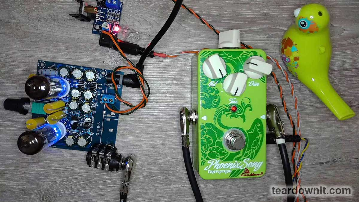 Connecting the Squier Bullet Mustang HH guitar directly to the amplifier, as well as through a homemade Landtone Phoenix Song Overdrive pedal (we have a separate post on it), https://youtu.be/kjpg-K5Ih_k The first sound test of this small amplifier made me smile. It has an unexpectedly pleasant, clean sound and a nice light overdrive. Higain, of course, will require additional equalization and power amp simulation. I will get my hands on sharp cutoff pentodes in the upcoming future and compare their sound as well as the oscillograms of sinusoidal signal processing. Thank you for your time! |
| json metadata | {"tags":["diy"],"image":["https://assets-global.website-files.com/6438c93ff266bb9903cab3bc/658d32b8447b358ca3ec004d_1.jpg","https://assets-global.website-files.com/6438c93ff266bb9903cab3bc/658d32ca18dfa9bfbf6bf437_2.jpg","https://cdn.steemitimages.com/DQmRwMgtNv2hbdA6yKteTrMvX8EPDjdoX7gWhcyp3FRCi8k/image.png","https://assets-global.website-files.com/6438c93ff266bb9903cab3bc/658d32df326525fa7f8d17ac_4.gif","https://cdn.steemitimages.com/DQmSEt3hM81N3GAB3qRHwNjzL1TaEU4xChm1fxxK3szmoqU/image.png","https://cdn.steemitimages.com/DQmbg4q7s84NgiX9vZeiLoJ7PeJku7Dbks7GUyXv9qTEx7c/image.png","https://cdn.steemitimages.com/DQmWpyRryTaUsqkZ3wGXYvdFJKXiSfEVoL2DBk8m7CkGsvE/image.png","https://cdn.steemitimages.com/DQmc7S7CZDm5X1rs9c6bPNGYEcUVJqxt3kZMW679F5sDfzz/image.png","https://cdn.steemitimages.com/DQmP5PabUxe3h7urKB7aQiu4XL6eyi8YsSxLvSeXnPZLHVc/image.png","https://assets-global.website-files.com/6438c93ff266bb9903cab3bc/658d331f14bd0e70461230e4_10.jpg","https://cdn.steemitimages.com/DQmceXX7tzofzgo3r2RDGamQqjjb5qVxwB39KsfqPaM2eDa/image.png","https://cdn.steemitimages.com/DQmbMTFgoXFPeS1GJauKp3Rf5kZrfZYNX1LjShMrw4S2uzN/image.png","https://assets-global.website-files.com/6438c93ff266bb9903cab3bc/658d333246a2dae05247b239_13.jpg","https://cdn.steemitimages.com/DQmNbPed82zy5VABzg1u4zeNTegQMPQmWWsPpR9wmknWFZe/image.png","https://img.youtube.com/vi/kjpg-K5Ih_k/0.jpg"],"links":["https://youtu.be/kjpg-K5Ih_k"],"app":"steemit/0.2","format":"markdown"} |
| parent author | |
| parent permlink | diy |
| permlink | simple-diy-tube-guitar-amplifier |
| title | Simple DIY tube guitar amplifier |
| Transaction Info | Block #81295414/Trx a0cf1de30b8a02cd7ca8916032ae3cfcdd64cffe |
View Raw JSON Data
{
"block": 81295414,
"op": [
"comment",
{
"author": "teardownit",
"body": "Vacuum tube technology always means bulky, heavy cases, dangerously high voltages, and complex multi-channel power supplies. Or does it?\n\nThis little amplifier is powered by a 12V wall-wart AC/AC transformer adapter. Its anode voltage is only 56 volts. It's high time to learn how this voltage is created from 12V and how a simple tube amp actually works.\n\nWe will also see on the oscilloscope screen that that unique tube sound signature is loved by audiophiles and musicians, especially guitarists. And then, we'll talk about the difference between long and short vacuum tubes.\n\nThe amplifier uses two 6BA6 pentodes. One can also use 6BD6, European EF93, and Chinese 6K4. In today's experiment, I specifically used 6K4s because they are inexpensive and easy to get.\n\nInstead of pentodes with long characteristics and long bodies, one can use short ones like 6AK5, EF95, 6J1, and 6J2. They will also sound great but in a different way.\nhttps://assets-global.website-files.com/6438c93ff266bb9903cab3bc/658d32b8447b358ca3ec004d_1.jpg\nTo understand the difference between a remote (long) cutoff and a sharp (short) cutoff of a vacuum tube, let’s check the principles of their operation.\n\nThe simplest vacuum tube is called a diode because it has two electrodes: a negative cathode and a positive anode. They are both contained in a glass or metal container with air pumped out of it so that its molecules do not interfere with the movement of electrons.\n\nThe silverish substance at the top of the flask is a gas absorber. It removes residual gas particles from the lamp that haven't been pumped out during the manufacturing process or those released due to heating.\nhttps://assets-global.website-files.com/6438c93ff266bb9903cab3bc/658d32ca18dfa9bfbf6bf437_2.jpg\nThe cathode is usually a nickel straw coated with barium or strontium oxide. The oxide coating is necessary to enhance electron emission.\n\nInside the tube, there is a heater—a tungsten spiral, like in an incandescent light bulb. The spiral is electrically isolated from the tube, which allows several tube heaters to be powered by a single source of current. The cathodes of those tubes can have different voltages and different signals at the same time.\n\nThe most common tubes are designed for heater voltages of 6.3 and 12.6 volts. The model numbers of American and Chinese tubes, unlike European ones, begin with one or two digits of the filament voltage. For example, 12AX7, 6BA6, and today's 6K4.\n\nThere are also directly heated cathodes, which are just tungsten spirals. They are typically used in battery-powered tubes. For example, 1N34, 2L34, and their Chinese analogs 1A2 and 2P2. This cathode is easier to heat and keep heated, which saves battery life.\n\nThe anode is usually a metal box covering the cathode. The anodes of low-power tubes are made of nickel or iron, and those of high-power ones are made of molybdenum, tantalum, or graphite, as they can withstand higher temperatures.\n\nThe surface of the anode is often made black and ribbed to radiate heat efficiently. The tube's electrode cannot transfer heat through convection because no air is around it.\n\nThe thermal conductivity of the electrode standoffs that complete the electrical loop to the output terminals is tiny. So, the only way to transfer heat from the inner parts to the outside environment is through thermal radiation.\n\n\n\nThe heated cathode emits electrons, and a cloud of electrons forming around it is called space charge. Like charges repel, space charge prevents further emission of electrons from the cathode.\n\nSuppose the anode has negative or zero potential relative to the cathode. In that case, nothing happens, and the current won't flow through the tube from the cathode to the anode. But, the positive potential of the anode attracts electrons. They will fly towards the anode, and the current will flow.\n\nThus, a vacuum diode allows current to flow in only one direction—from the anode to the cathode. After all, the direction of the current is always indicated by an arrow from plus to minus; this direction is for the movement of imaginary positive charges.\n\nIn P-type semiconductors, charge carriers are indeed positive; in electrolytes, both positive and negative; and in metal wires and vacuum tubes, negative electrons.\n\nSo, a vacuum diode can be used for rectifying AC current (then the tube is called a kenotron), detecting an amplitude-modulated radio signal, and for many other purposes where current needs to be passed in only one direction.\n\nThings get much more enjoyable when, between the cathode and anode, the mesh is added. Such a tube with three different electrodes is called a triode.\n\nhttps://assets-global.website-files.com/6438c93ff266bb9903cab3bc/658d32df326525fa7f8d17ac_4.gif\nWhen the mesh is negatively charged relative to the cathode, it repels electrons. It makes it harder for them to reach the anode until the flow is completely blocked.\n\nWhen the mesh's potential is positive relative to the cathode, it attracts electrons from the cathode. Some electrons are captured by the mesh wires and never reach the anode. They create a grid current, a very small one because the wires are thin and the gaps between them are huge.\n\nTherefore, most of the electrons attracted from the cathode and accelerated by the positive potential of the mesh fly right through it and reach the anode. The anode current is much greater than the mesh current.\n\nHowever, any tube circuitry must have a so-called grid leak, an electrical loop, usually just a resistor between the mesh and the cathode, ensuring the return of electrons from the grid to the cathode. Otherwise, electrons will accumulate on the insulated mesh, and a significant negative potential will occur, which will block the lamp.\n\nSo, a vacuum triode is a device that controls the anode current by changing the grid voltage. Suppose a resistance is included in the anode or cathode circuit. In that case, the voltage drop across it will correspond to the anode (or cathode) current according to Ohm’s law.\n\nThus, we get an amplification of voltage, current, and power. A small change in grid voltage with a tiny grid current controls significant changes in output voltage and current.\n\nThis way, one can amplify the signal from a microphone, the pickup of a vinyl record player or guitar, radio waves from an antenna, and so on. And if a transformer with a loudspeaker is connected to the anode circuit, we get a loud-speaking sound amplifier.\n\nThe usual mesh of a regular \"short\" tube has an equal distance between the wires. Or should we say coils because the wires are actually coils winded around the mesh posts.\n\n\n\nThe image shows how the negative potential of the grid shields the positive electric field of the anode, preventing it from attracting electrons from the cathode.\n\nThe mesh of the “long” tube is wound unevenly, with different distances between the turns. And this is not a sign of carelessness; it was done intentionally.\n\n\n\nIn those places where the distance between the wires is wider, the electric field of the anode does not immediately switch to the grid. Still, it continues to reach the cathode, attracting electrons. This allows for the extension of the characteristic of the tube, which is the main difference between a remote (long) cutoff and a sharp (short) cutoff.\n\n\nWhat is the nonlinear transfer characteristic of the tube needed for? Doesn't it distort the signal? And the answer is yes, it distorts, and when applied to guitar amplification and music reproduction, this helps to get interesting results.\n\nHowever, remote cutoff tubes were originally intended for circuits with automatic gain control. The dependence of the amplification factor, or µ (Greek letter \"mu\"), on the grid bias voltage, allows one to make a voltage-controlled amplifier (VCA).\n\nAnd suppose this offset is set by an amplitude envelope detector (like the one in VU-meters). In that case, we get greater amplification of the strong signal and less amplification of the weak one, that is, compression and stabilization of the signal level. This can be very useful and necessary in many cases.\n\nSo, let's get started with our amplifier. I took a popular tube buffer board for a home audio system as a base for my project; only a couple of modifications were needed. Here is the diagram for this board.\n\n\n\n\nThe amplifier consists of two identical stages. Pentodes here are used as triodes; the second mesh is connected to the anode. The tubes are connected according to a common-cathode circuit.\n\nR13, R18—grid leak resistance. R14, R19—cathode bias resistances, providing a negative grid potential relative to the cathode. R15 and R20 are anode load resistors outputting the amplified signal.\n\nThe cathode heaters are connected in series since the supply voltage of the circuit is 12 volts alternating current, and the nominal filament voltage of each lamp is 6.3 volts, so the total is 12.6 volts.\n\nIn this scheme, the heaters are powered by a smoothed direct current. This is an ideal way to power them because it eliminates the possibility of AC mains hum remaining in the output signal.\n\nThe voltage for powering the heaters is provided by a half-wave rectifier D1 and a pulsation-smoothing RC filter R1 C13 after it.\n\nThe tubes are beautifully illuminated by blue LEDs (LED1 and LED2). Since LEDs cannot withstand reverse voltage, they are powered by direct current from the filament rectifier D1. R10 and R11 determine the LED current.\n\nAn anode supply of 56 volts is obtained using voltage quadruples consisting of two doublers: positive voltage +28V D2, D3, C1, C2, and negative voltage -28V D4, D5, C5, C6.\n\nTwo capacitance multipliers are assembled on capacitors C3 and C7 and transistors TR1 and TR3. Another name for such a circuit is an electronic choke.\n\nThe capacitance multiplier is an emitter follower with a capacitor at its input. At the output, the repeater will maintain a constant voltage smoothed by a capacitor.\n\nThus, the capacitance of the capacitor is multiplied by the transistor gain plus one, β + 1. The minimum gain of the 2SD667A-C and 2SB647A-C transistors is 100.\n\nThanks to the capacitance multiplier, we have the equivalent of filter capacitors with a capacity of over 4700 microfarads. This ensures almost perfect filtration of the anode power.\n\nCurrent limiters are assembled on transistors TR2 and TR4. Suppose the voltage across the resistor R4, through which the anode current flows, reaches a value sufficient to open TR2. In that case, it opens and bypasses the base junction of TR1, closing it.\n\nCurrent protection TR4 R8 works in precisely the same way. And resistors R5 and R9 form additional RC filters with capacitors C4 and C8.\n\nTo get a two-stage monophonic guitar amplifier from a single-stage stereo amplifier, connect the left channel output to the right channel volume control input.\n\nApply a sinusoidal signal with a frequency of 500–3000 Hz to the input of the amplifier, and you'll see a pure sine wave on the oscilloscope screen.\n\n\nIncreasing the signal level, we widen the upper half-wave and narrow the lower half-wave.\n\nhttps://assets-global.website-files.com/6438c93ff266bb9903cab3bc/658d331f14bd0e70461230e4_10.jpg\nThis waveform is characteristic of the sum of a sine signal with its second harmonic, the same sinusoid, but with double the frequency and half the amplitude.\n\n\n These even harmonics are the secret to the beauty of the tube sound that we adore so much. They can be obtained without a tube by digital or analog simulation. Still, in tube stages, they arise naturally with no trickery.\n\nThe amplifier board was originally intended to act as a buffer between components in a home stereo system. That is, to match the high output impedance of a signal source (for example, a player) with the low input impedance of a receiver (for example, an amplifier).\n\nIt also eliminates the influence of connecting cables. It slightly enriches the signal with tube harmonics, which add crispness and beauty to the sound of individual instruments in a composition. High gain is not required from such a tube buffer; the signal level at both the input and output is linear.\n\nI will use the amplifier as a guitar one, so I'll solder a couple of 100 uF 16V capacitors in parallel with the cathode resistors R14 and R19, positive terminals to the cathode of the lamp.\n\nThis will ground the cathodes for AC without changing the DC bias. The gain of the amplifier will increase.\n\n\nNow, when the volume control knob comes close to the right-most position, the upper half-wave acquires a flat top with no sharp bends, indicating a soft tube limitation.\n\nThe tube preamp is ready for testing. As a power amplifier, we will use a board based on the TDA2030 chip in standard configuration as an electronic load with Cabsim, Torpedo Captor X.\nhttps://assets-global.website-files.com/6438c93ff266bb9903cab3bc/658d333246a2dae05247b239_13.jpg\n\n\n\nConnecting the Squier Bullet Mustang HH guitar directly to the amplifier, as well as through a homemade Landtone Phoenix Song Overdrive pedal (we have a separate post on it),\nhttps://youtu.be/kjpg-K5Ih_k\nThe first sound test of this small amplifier made me smile. It has an unexpectedly pleasant, clean sound and a nice light overdrive. Higain, of course, will require additional equalization and power amp simulation.\n\nI will get my hands on sharp cutoff pentodes in the upcoming future and compare their sound as well as the oscillograms of sinusoidal signal processing.\n\nThank you for your time!",
"json_metadata": "{\"tags\":[\"diy\"],\"image\":[\"https://assets-global.website-files.com/6438c93ff266bb9903cab3bc/658d32b8447b358ca3ec004d_1.jpg\",\"https://assets-global.website-files.com/6438c93ff266bb9903cab3bc/658d32ca18dfa9bfbf6bf437_2.jpg\",\"https://cdn.steemitimages.com/DQmRwMgtNv2hbdA6yKteTrMvX8EPDjdoX7gWhcyp3FRCi8k/image.png\",\"https://assets-global.website-files.com/6438c93ff266bb9903cab3bc/658d32df326525fa7f8d17ac_4.gif\",\"https://cdn.steemitimages.com/DQmSEt3hM81N3GAB3qRHwNjzL1TaEU4xChm1fxxK3szmoqU/image.png\",\"https://cdn.steemitimages.com/DQmbg4q7s84NgiX9vZeiLoJ7PeJku7Dbks7GUyXv9qTEx7c/image.png\",\"https://cdn.steemitimages.com/DQmWpyRryTaUsqkZ3wGXYvdFJKXiSfEVoL2DBk8m7CkGsvE/image.png\",\"https://cdn.steemitimages.com/DQmc7S7CZDm5X1rs9c6bPNGYEcUVJqxt3kZMW679F5sDfzz/image.png\",\"https://cdn.steemitimages.com/DQmP5PabUxe3h7urKB7aQiu4XL6eyi8YsSxLvSeXnPZLHVc/image.png\",\"https://assets-global.website-files.com/6438c93ff266bb9903cab3bc/658d331f14bd0e70461230e4_10.jpg\",\"https://cdn.steemitimages.com/DQmceXX7tzofzgo3r2RDGamQqjjb5qVxwB39KsfqPaM2eDa/image.png\",\"https://cdn.steemitimages.com/DQmbMTFgoXFPeS1GJauKp3Rf5kZrfZYNX1LjShMrw4S2uzN/image.png\",\"https://assets-global.website-files.com/6438c93ff266bb9903cab3bc/658d333246a2dae05247b239_13.jpg\",\"https://cdn.steemitimages.com/DQmNbPed82zy5VABzg1u4zeNTegQMPQmWWsPpR9wmknWFZe/image.png\",\"https://img.youtube.com/vi/kjpg-K5Ih_k/0.jpg\"],\"links\":[\"https://youtu.be/kjpg-K5Ih_k\"],\"app\":\"steemit/0.2\",\"format\":\"markdown\"}",
"parent_author": "",
"parent_permlink": "diy",
"permlink": "simple-diy-tube-guitar-amplifier",
"title": "Simple DIY tube guitar amplifier"
}
],
"op_in_trx": 0,
"timestamp": "2024-01-03T07:48:18",
"trx_id": "a0cf1de30b8a02cd7ca8916032ae3cfcdd64cffe",
"trx_in_block": 1,
"virtual_op": 0
}bluesnipersent 0.010 STEEM to @teardownit- "Hello. Good to see you on Steem. To maximize your rewards, publish your post also on Hive ( hive.blog ) and Blurt ( blurt.blog ) blockchains. Use upvu, jsup or ctime and get instant upvotes"2023/12/20 07:37:21
bluesnipersent 0.010 STEEM to @teardownit- "Hello. Good to see you on Steem. To maximize your rewards, publish your post also on Hive ( hive.blog ) and Blurt ( blurt.blog ) blockchains. Use upvu, jsup or ctime and get instant upvotes"
2023/12/20 07:37:21
| amount | 0.010 STEEM |
| from | bluesniper |
| memo | Hello. Good to see you on Steem. To maximize your rewards, publish your post also on Hive ( hive.blog ) and Blurt ( blurt.blog ) blockchains. Use upvu, jsup or ctime and get instant upvotes |
| to | teardownit |
| Transaction Info | Block #80894343/Trx 191b4bfbc94e5f0daf42aaa10c2548b02f2fbb2a |
View Raw JSON Data
{
  "block": 80894343,
  "op": [
    "transfer",
    {
      "amount": "0.010 STEEM",
      "from": "bluesniper",
      "memo": "Hello. Good to see you on Steem. To maximize your rewards, publish your post also on Hive ( hive.blog ) and Blurt ( blurt.blog ) blockchains. Use upvu, jsup or ctime and get instant upvotes",
      "to": "teardownit"
    }
  ],
  "op_in_trx": 0,
  "timestamp": "2023-12-20T07:37:21",
  "trx_id": "191b4bfbc94e5f0daf42aaa10c2548b02f2fbb2a",
  "trx_in_block": 0,
  "virtual_op": 0
}bluesniperupvoted (100.00%) @teardownit / pcb-assembly-desktop-factory-project-our-team2023/12/20 07:36:57
bluesniperupvoted (100.00%) @teardownit / pcb-assembly-desktop-factory-project-our-team
2023/12/20 07:36:57
| author | teardownit |
| permlink | pcb-assembly-desktop-factory-project-our-team |
| voter | bluesniper |
| weight | 10000 (100.00%) |
| Transaction Info | Block #80894335/Trx 1aa2236eb66c8a3c46c462cb3b99a2bf9030cb30 |
View Raw JSON Data
{
  "block": 80894335,
  "op": [
    "vote",
    {
      "author": "teardownit",
      "permlink": "pcb-assembly-desktop-factory-project-our-team",
      "voter": "bluesniper",
      "weight": 10000
    }
  ],
  "op_in_trx": 0,
  "timestamp": "2023-12-20T07:36:57",
  "trx_id": "1aa2236eb66c8a3c46c462cb3b99a2bf9030cb30",
  "trx_in_block": 1,
  "virtual_op": 0
}teardownitpublished a new post: pcb-assembly-desktop-factory-project-our-team2023/12/20 07:31:30
teardownitpublished a new post: pcb-assembly-desktop-factory-project-our-team
2023/12/20 07:31:30
| author | teardownit |
| body | We have many years of experience in developing electronic devices for various customers. When we complete a non-standard task, we often explore new methods and ways to achieve the required result. By accumulating this knowledge, we create solutions to simplify the design and creation of devices. It's time to share some of our solutions with the community now. https://assets-global.website-files.com/6438c93ff266bb9903cab3bc/657999f43af2127dbf852dd0_1.jpg Core team: • 3 full-time hard/firmware engineers • 15-30 years in product R&D and systems engineering • full range of product development jobs: - highlighting the problem - transforming it into a task - searching for possible solutions based on target parameters - analysis and selection of the best option Application and system programming: • core team programming languages: C/C++, ASM • compilers: C /C++ (CLI): GCC, IAR, SDCC, C++ Builder, Avocet C, Hi-Tech C • IDE: SlickEdit, emacs, IAR Embedded Workbench, Multi-Edit, eclipse cdt, STM32CubeIDE, Atmel Start, Atmel Studio, NetBeans IDE, Qt Creator • make, cmake, qmake, cvs, subversion, git, etc • experience/projects: - embedded programming z80, MCS-51, AVR, PIC, ARM (7, 9, Cortex), STM8 - RT-tasks under eCos - eCos modules - in-house RTOS for telecom equipment - special Windows-NT services for own hardware - BDOS/BIOS CP/M for Z80CPU hardware emulator - desktop applications for Windows/Linux Circuit engineering: • analog: automation, data acquisition, measurements, sound, etc • digital: from simple logic circuits to FPGA/MCU/PSoC • power electronics: experience in DC/DC up to 600W • experience: PSpice, VHDL, Verilog Electronic devices R&D: • PCB/PCBA TH/SMD/multilayer w/auto testing @ production cycle • PCBA (bare and cased) thermal calculations • calculation and design of pulse transformers and inductors • 3D housing design • experience: KiCAD, Altium Designer, FreeCAD, OpenSCAD, Fusion360 projects: - wide spectrum of microcontrollers - telecommunication equipment (about 1M subscribers in service) - time measurement equipment for telecom - hardware emulator with a signature analyzer |
| json metadata | {"tags":["pcb"],"image":["https://assets-global.website-files.com/6438c93ff266bb9903cab3bc/657999f43af2127dbf852dd0_1.jpg"],"app":"steemit/0.2","format":"markdown"} |
| parent author | |
| parent permlink | pcb |
| permlink | pcb-assembly-desktop-factory-project-our-team |
| title | PCB Assembly Desktop Factory project. Our team |
| Transaction Info | Block #80894227/Trx 1448e26cfc15c395c976c96d8b4fe985ad5bc764 |
View Raw JSON Data
{
"block": 80894227,
"op": [
"comment",
{
"author": "teardownit",
"body": "We have many years of experience in developing electronic devices for various customers. When we complete a non-standard task, we often explore new methods and ways to achieve the required result. By accumulating this knowledge, we create solutions to simplify the design and creation of devices. It's time to share some of our solutions with the community now.\n\nhttps://assets-global.website-files.com/6438c93ff266bb9903cab3bc/657999f43af2127dbf852dd0_1.jpg\n\nCore team:\n• 3 full-time hard/firmware engineers\n• 15-30 years in product R&D and systems engineering\n• full range of product development jobs:\n- highlighting the problem\n- transforming it into a task\n- searching for possible solutions based on target parameters\n- analysis and selection of the best option\n\n\nApplication and system programming:\n• core team programming languages: C/C++, ASM\n• compilers: C /C++ (CLI): GCC, IAR, SDCC, C++ Builder, Avocet C, Hi-Tech C\n• IDE: SlickEdit, emacs, IAR Embedded Workbench, Multi-Edit, eclipse cdt, STM32CubeIDE, Atmel Start, Atmel Studio, NetBeans IDE, Qt Creator\n• make, cmake, qmake, cvs, subversion, git, etc\n• experience/projects:\n- embedded programming z80, MCS-51, AVR, PIC, ARM (7, 9, Cortex), STM8\n- RT-tasks under eCos\n- eCos modules\n- in-house RTOS for telecom equipment\n- special Windows-NT services for own hardware\n- BDOS/BIOS CP/M for Z80CPU hardware emulator\n- desktop applications for Windows/Linux\n\n\nCircuit engineering:\n• analog: automation, data acquisition, measurements, sound, etc\n• digital: from simple logic circuits to FPGA/MCU/PSoC\n• power electronics: experience in DC/DC up to 600W\n• experience: PSpice, VHDL, Verilog\n\n\nElectronic devices R&D:\n• PCB/PCBA TH/SMD/multilayer w/auto testing @ production cycle\n• PCBA (bare and cased) thermal calculations\n• calculation and design of pulse transformers and inductors\n• 3D housing design\n• experience: KiCAD, Altium Designer, FreeCAD, OpenSCAD, Fusion360\nprojects:\n- wide spectrum of microcontrollers\n- telecommunication equipment (about 1M subscribers in service)\n- time measurement equipment for telecom\n- hardware emulator with a signature analyzer",
"json_metadata": "{\"tags\":[\"pcb\"],\"image\":[\"https://assets-global.website-files.com/6438c93ff266bb9903cab3bc/657999f43af2127dbf852dd0_1.jpg\"],\"app\":\"steemit/0.2\",\"format\":\"markdown\"}",
"parent_author": "",
"parent_permlink": "pcb",
"permlink": "pcb-assembly-desktop-factory-project-our-team",
"title": "PCB Assembly Desktop Factory project. Our team"
}
],
"op_in_trx": 0,
"timestamp": "2023-12-20T07:31:30",
"trx_id": "1448e26cfc15c395c976c96d8b4fe985ad5bc764",
"trx_in_block": 6,
"virtual_op": 0
}davidesimonciniupvoted (12.80%) @teardownit / diy-functional-oscillators2023/12/14 07:52:21
davidesimonciniupvoted (12.80%) @teardownit / diy-functional-oscillators
2023/12/14 07:52:21
| author | teardownit |
| permlink | diy-functional-oscillators |
| voter | davidesimoncini |
| weight | 1280 (12.80%) |
| Transaction Info | Block #80722517/Trx 1842cd8368ea636ef96d2ff779cfd2d309980a51 |
View Raw JSON Data
{
  "block": 80722517,
  "op": [
    "vote",
    {
      "author": "teardownit",
      "permlink": "diy-functional-oscillators",
      "voter": "davidesimoncini",
      "weight": 1280
    }
  ],
  "op_in_trx": 0,
  "timestamp": "2023-12-14T07:52:21",
  "trx_id": "1842cd8368ea636ef96d2ff779cfd2d309980a51",
  "trx_in_block": 3,
  "virtual_op": 0
}teardownitpublished a new post: diy-functional-oscillators2023/12/14 07:49:57
teardownitpublished a new post: diy-functional-oscillators
2023/12/14 07:49:57
| author | teardownit |
| body | https://assets-global.website-files.com/6438c93ff266bb9903cab3bc/656f175795975764f97eec63_0.jpg Signal distortion induced by electronic devices, primarily amplifiers, could be either undesirable or useful. When we play back an audio recording, we want it to sound as close to the original as possible. Or sometimes, we want to add just a smidge of tube distortion. On the other hand, magnetic recording on tape and mechanical recording on vinyl, by their nature, significantly alter the sound; therefore, distortions are deliberately added into the circuits of recorders and playback equipment so that, in the end, the resulting audio signal turns out to be indistinguishable from what has been recorded. In addition, volume controls are equipped with loudness compensation to account for human hearing abilities. Mobile pocket audio devices have tiny speakers, and their power amplifiers are specifically designed to add bass and limit treble so that the sound is deeper and less squeaky. Multi-way speaker systems have filters, and sometimes even separate amplifiers, that slice the sound signal into frequency bands for each dedicated speaker: subwoofer, low-frequency, mid-frequency, and tweeter. These can also be considered deliberately created distortions. Finally, processing an electric guitar signal requires numerous fine-tuned distortions. They form a wonderful guitar tone. But if we simply plug the best electric guitar into a hi-fi amplifier, we'll be disappointed. One can also identify a malfunction by the specific distortions of the signal and, by tracking the signal flow, specify the location of the malfunction in a complex circuit. A device that allows you to see distortions is called an oscilloscope. But having an oscilloscope is not enough; we will also need a standard waveform signal generator. Today, we will assemble three such generators. So-called standard waveforms are sine, triangle, and square. Devices that generate such signals are called function generators. A sine wave is the simplest signal, but it is the most difficult to create without an LC resonant tank, using only RC circuits. A pure sine wave oscillates one frequency; it is needed to determine the harmonics the circuit adds to the signal. https://assets-global.website-files.com/6438c93ff266bb9903cab3bc/656f175f8e08a1310d2958eb_1.jpg For example, in this image from the post about the tube amplifier, we see that the upper half-wave is wide and rounded, and the lower half-wave is narrow and pointy. This indicates the presence of a second harmonic, which makes tube amplifiers sound so beautiful. 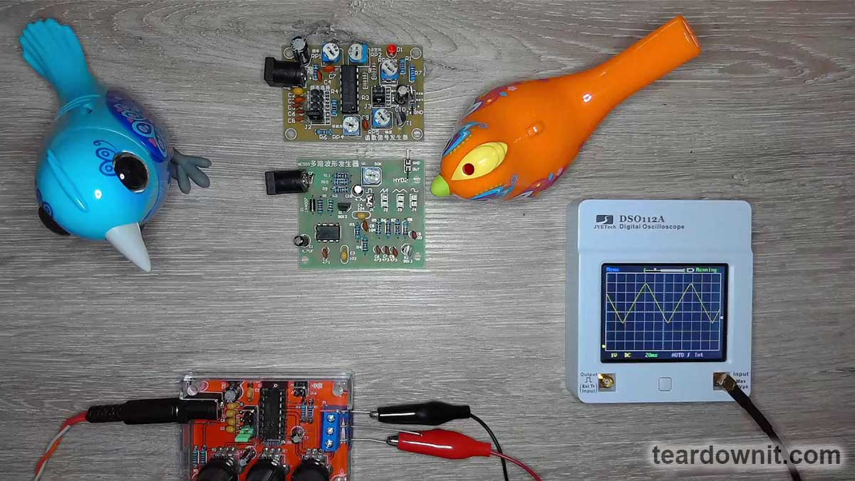 A triangular waveform could be created by a ramp voltage generator. Such a signal allows one to see nonlinear distortions as lines bend on the oscilloscope screen. https://assets-global.website-files.com/6438c93ff266bb9903cab3bc/656f176ecd6fdc7a855d50a4_3.jpg Bending them a certain way brings the triangle line closer to a sinusoid. This is exactly how the function generators on microchips that we are studying today are designed. https://assets-global.website-files.com/6438c93ff266bb9903cab3bc/656f177410ed478c8d71d397_4.jpg An ideal square wave consists of vertical and horizontal lines. Looking at the flow of such a signal, one can see the frequency-dependent deviations, interference, and parasitic processes. https://assets-global.website-files.com/6438c93ff266bb9903cab3bc/656f177b23efeb5e65958570_5.jpg For example, a differentiating circuit with a time constant of an order of magnitude smaller than the period of the input signal creates a sharp peak at the beginning of the horizontal section. https://assets-global.website-files.com/6438c93ff266bb9903cab3bc/656f1781d0bee6b070bd5910_6.jpg And this is what the result of the operation of an integrating circuit with a time constant comparable to the signal period looks like. https://assets-global.website-files.com/6438c93ff266bb9903cab3bc/656f17935ac0b0761beadb08_7.jpg If the integrator time constant is noticeably smaller than the signal period, then only the leading edges become sloped, and the top part of the square wave remains flat. In this oscillogram, we see additional high-frequency interference. https://assets-global.website-files.com/6438c93ff266bb9903cab3bc/656f179be13dfb1aef22ae6a_8.jpg Here, we see not just high-frequency noise but damping oscillations excited by sudden changes in the input signal. Such vibrations are called "ringing". Function generator on the XR2206 chip Our first generator can produce electrical oscillations with frequencies ranging from 1 Hz to 1 MHz. This is more than enough for an amateur's lab. https://assets-global.website-files.com/6438c93ff266bb9903cab3bc/656f17a3cbcf97095aefbee7_9.jpg The 300 kHz square wave we have here is distorted not by the generator itself but by the DSO112A oscilloscope, whose analog bandwidth is 2 MHz. https://assets-global.website-files.com/6438c93ff266bb9903cab3bc/656f17aaddf8c422e2ba477c_10.jpg At 20 kHz, the upper limit of the audible range, the square waveform appears almost perfect. https://assets-global.website-files.com/6438c93ff266bb9903cab3bc/656f17b1d0bee6b070bd9a2d_11.jpg The generator volume knob allows one to crank it up to the limiter. This generator feature must be kept in mind, or the limitation may sometimes seem to occur in the circuit under study. https://assets-global.website-files.com/6438c93ff266bb9903cab3bc/656f17b74eedf9867f6be68d_12.jpg The 400 kHz sine wave looks great. Remember that this is 1/5 of the oscilloscope's bandwidth, so all the harmonics higher than the fifth won't pass through the oscilloscope's analog input. This is a triangular waveform at a frequency of 130 kHz. The tops are slightly rounded, but the lines are straight. Everything looks as it should. The generator circuit is elementary. Capacitors C1 and C2 together are a power filter. The square wave output is pulled up by resistor R1 to the power supply positive because it is an open collector output. 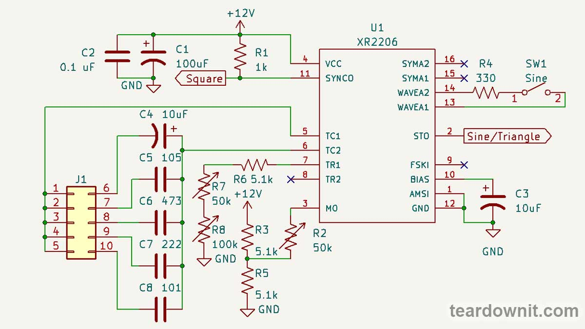 C4-C8 are timing capacitors, and J1 is their frequency range switch. Timing resistance is made up of three series resistors. R8 is a coarse frequency setting, R7 is a fine setting, and R6 is a limiting resistor, so it cannot be zero. The circuit has input 8 (TR2) for the second timing resistor. Pull pin 9 (FSKI) to the ground; input 8 (TR2) will become active. If input 8 is left disconnected or pulled to the power supply positive, then input 7 (TR1) is active. This option allows one to instantly switch between two oscillation periods, which is helpful for frequency shift keying or pulse width modulation. To get PWM, one needs to connect input 9 (FSKI) to output 11 (SYNCO). Then, the duty cycle will be determined by the ratio of the resistances connecting TR1 and TR2 to the ground, and the frequency will be determined by the sum of these resistances. Pin 3 (MO) bias setting is the gain adjustment. It is the amplitude of the output signal and is tweaked with a variable resistor, R2. Pins 13 and 14 (WAVEA1, WAVEA2) are used to form a sinusoid. Output 2 (STO) produces a triangle waveform if they are open. If those pins are connected through a resistor, there will be a sine wave. Its shape can be adjusted by changing the resistance R4. Input 1 (AMSI) is intended for amplitude modulation. We don't use it in this scheme. Output 10 (BIAS) is connected to the internal reference voltage source. To ensure its stability and the absence of any interference, a capacitor C3 is connected to it. You can add a potentiometer to pins 15 and 16 (SYMA1 and SYMA2) and connect its wiper to the ground. Then, it will be possible to further adjust the symmetry of the sinusoid. Although, as we've seen, this is optional. Function generator on the ICL8038 chip The ICL8038 chip has much in common with the XR2206; it is also designed to create a function generator with minimum external components. https://assets-global.website-files.com/6438c93ff266bb9903cab3bc/656f17cc7abe6bd44019db56_15.jpg Like the XR2206, the ICL8038 has a timing capacitor on input 9 (TIME_CAP). We switch through five different capacitors to get five frequency ranges. Square wave output 9 (SQR_OUT) for both microcircuits is an open collector. It needs to be pulled up to the positive power supply. ICL8038 has separate sine and triangle outputs: 2 (SINE_OUT) and 3 (TRI_OUT). The ICL8038 has only one input for timing resistor 8 (FM SWEEP), so we won't be able to switch between resistors and get FSK. 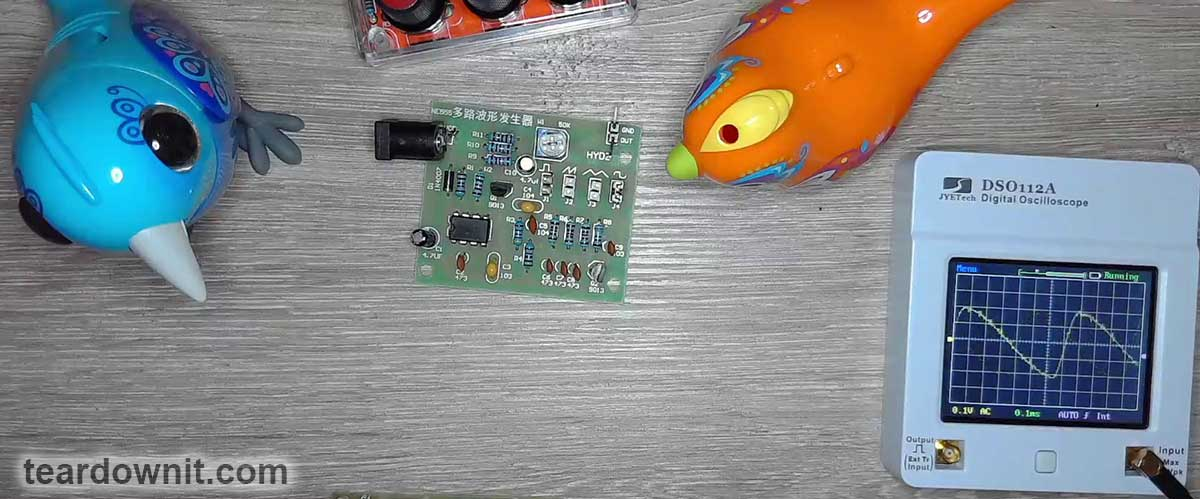 But inputs 4 and 5 allow one to adjust the duty cycle of PWM. The resistances between these pins and the power supply positive, set by the position of wiper RV2, affect all three outputs. 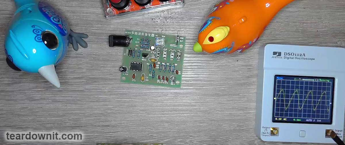 Resistor RV4, the bias of input 1 (SINE_ADJ), tweaks the vertical symmetry of the sine wave. As we already know, this affects the harmonic series of the signal. Simple function generator on NE555 If you do not have a specialized chip, a simple square, triangle, and sine wave generator can be assembled in many ways, for example, on a 555 timer. We see an emitter follower on transistor Q1 at the device's output. It has a positive bias in the form of resistor R10. The input resistance of this stage is about 100 kOhm, so the voltage at the base of Q1 will be about half the supply voltage. 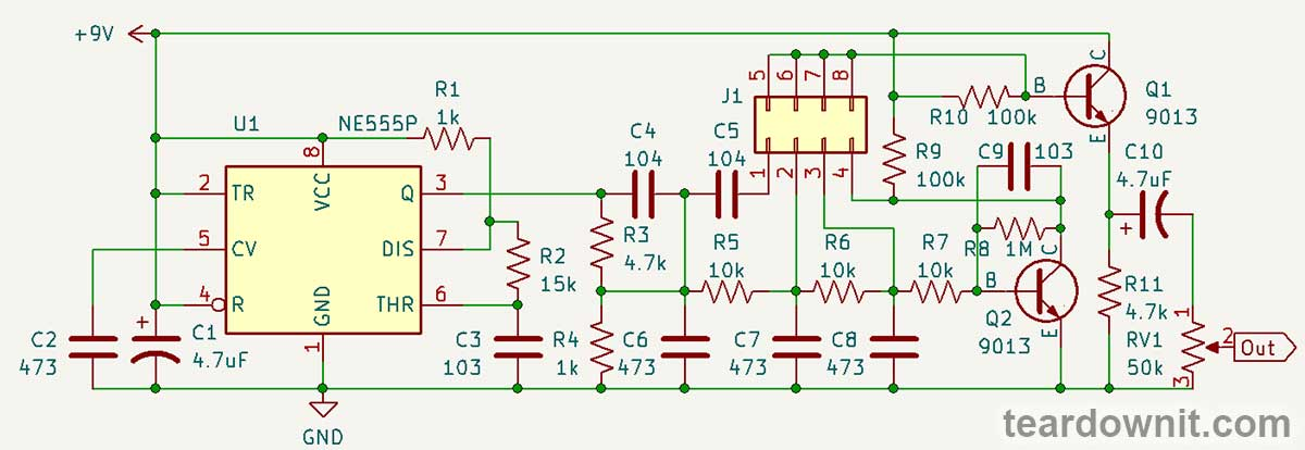 In the first position of the switch, rectangular pulses from the output of the 555 timers pass through series capacitors C4 and C5 and parallel capacitor C6. Resistor R3 is connected with C4, and R4 is connected in parallel with C6. The result is a hybrid of a rectangle and a ramp with decent linearity. One can evaluate the distortion and parasitic oscillations it introduces by comparing the original waveform with what is produced in a particular circuit. Next comes the integrator R5C7, after which crescent-shaped relaxation oscillations are obtained. The authors labeled this waveform a sawtooth or ramp, but it's more like shark fins. https://assets-global.website-files.com/6438c93ff266bb9903cab3bc/656f180d352bb3d0c014b2a9_21.jpg After the second similar integrator, R6C8, a hybrid of a triangle and a sine wave is created: the tops are rounded, but the inclined sections are almost linear. https://assets-global.website-files.com/6438c93ff266bb9903cab3bc/656f18128c47ca68d9deb820_22.jpg And finally, after the transistor stage on Q2, shunted by capacitor C9, we get an excellent approximation of a sinusoid. Resistor R8 provides base bias to Q2. So we've seen what capacitors, resistors, and a transistor do to an electrical signal, and we learned how to build a simple generator with recognizable waveforms that can be used to study distortions in electrical circuits. It is not that difficult to assemble a proper function generator on a special microcircuit. Still, it will definitely have more functions and better signal quality. Professional-grade devices are, of course, more advanced, but they have a much higher price and substantially bigger dimensions. Unlike the three simple generators we've assembled and tested today, not every electronics enthusiast can afford them. https://youtu.be/N6ce_Y_GoPA |
| json metadata | {"tags":["diyelectronics"],"image":["https://assets-global.website-files.com/6438c93ff266bb9903cab3bc/656f175795975764f97eec63_0.jpg","https://assets-global.website-files.com/6438c93ff266bb9903cab3bc/656f175f8e08a1310d2958eb_1.jpg","https://cdn.steemitimages.com/DQmUjjyrFqJi79ivahtgCJTjEMaHMJuVxXYKE54vytDfQ1N/image.png","https://assets-global.website-files.com/6438c93ff266bb9903cab3bc/656f176ecd6fdc7a855d50a4_3.jpg","https://assets-global.website-files.com/6438c93ff266bb9903cab3bc/656f177410ed478c8d71d397_4.jpg","https://assets-global.website-files.com/6438c93ff266bb9903cab3bc/656f177b23efeb5e65958570_5.jpg","https://assets-global.website-files.com/6438c93ff266bb9903cab3bc/656f1781d0bee6b070bd5910_6.jpg","https://assets-global.website-files.com/6438c93ff266bb9903cab3bc/656f17935ac0b0761beadb08_7.jpg","https://assets-global.website-files.com/6438c93ff266bb9903cab3bc/656f179be13dfb1aef22ae6a_8.jpg","https://assets-global.website-files.com/6438c93ff266bb9903cab3bc/656f17a3cbcf97095aefbee7_9.jpg","https://assets-global.website-files.com/6438c93ff266bb9903cab3bc/656f17aaddf8c422e2ba477c_10.jpg","https://assets-global.website-files.com/6438c93ff266bb9903cab3bc/656f17b1d0bee6b070bd9a2d_11.jpg","https://assets-global.website-files.com/6438c93ff266bb9903cab3bc/656f17b74eedf9867f6be68d_12.jpg","https://cdn.steemitimages.com/DQmW6enVtjQDagLy8TSVPc1vDMLz8imdtTsAWM4UdcZ8e4g/image.png","https://assets-global.website-files.com/6438c93ff266bb9903cab3bc/656f17cc7abe6bd44019db56_15.jpg","https://cdn.steemitimages.com/DQmUFik9UcaLAzaQLqChAA7kt1CXxWw81fPMvK4tTJxD97u/image.png","https://cdn.steemitimages.com/DQmcEP8ezmMpET21keP5oePFbzCVL2ZBDjQsQzGkXTGkqFZ/image.png","https://cdn.steemitimages.com/DQmaADoDC7qfCDgoAijbgCPwpRwoZm3M3wZvPm3CTDPGxEz/image.png","https://assets-global.website-files.com/6438c93ff266bb9903cab3bc/656f180d352bb3d0c014b2a9_21.jpg","https://assets-global.website-files.com/6438c93ff266bb9903cab3bc/656f18128c47ca68d9deb820_22.jpg","https://img.youtube.com/vi/N6ce_Y_GoPA/0.jpg"],"links":["https://youtu.be/N6ce_Y_GoPA"],"app":"steemit/0.2","format":"markdown"} |
| parent author | |
| parent permlink | diyelectronics |
| permlink | diy-functional-oscillators |
| title | DIY functional oscillators |
| Transaction Info | Block #80722469/Trx f9051ab8db26919db318de9b7b5add300e872042 |
View Raw JSON Data
{
"block": 80722469,
"op": [
"comment",
{
"author": "teardownit",
"body": "https://assets-global.website-files.com/6438c93ff266bb9903cab3bc/656f175795975764f97eec63_0.jpg\n\nSignal distortion induced by electronic devices, primarily amplifiers, could be either undesirable or useful.\n\nWhen we play back an audio recording, we want it to sound as close to the original as possible. Or sometimes, we want to add just a smidge of tube distortion.\n\nOn the other hand, magnetic recording on tape and mechanical recording on vinyl, by their nature, significantly alter the sound; therefore, distortions are deliberately added into the circuits of recorders and playback equipment so that, in the end, the resulting audio signal turns out to be indistinguishable from what has been recorded.\n\nIn addition, volume controls are equipped with loudness compensation to account for human hearing abilities.\n\nMobile pocket audio devices have tiny speakers, and their power amplifiers are specifically designed to add bass and limit treble so that the sound is deeper and less squeaky.\n\nMulti-way speaker systems have filters, and sometimes even separate amplifiers, that slice the sound signal into frequency bands for each dedicated speaker: subwoofer, low-frequency, mid-frequency, and tweeter. These can also be considered deliberately created distortions.\n\nFinally, processing an electric guitar signal requires numerous fine-tuned distortions. They form a wonderful guitar tone. But if we simply plug the best electric guitar into a hi-fi amplifier, we'll be disappointed.\n\nOne can also identify a malfunction by the specific distortions of the signal and, by tracking the signal flow, specify the location of the malfunction in a complex circuit.\n\nA device that allows you to see distortions is called an oscilloscope. But having an oscilloscope is not enough; we will also need a standard waveform signal generator. Today, we will assemble three such generators.\n\nSo-called standard waveforms are sine, triangle, and square. Devices that generate such signals are called function generators.\n\nA sine wave is the simplest signal, but it is the most difficult to create without an LC resonant tank, using only RC circuits. A pure sine wave oscillates one frequency; it is needed to determine the harmonics the circuit adds to the signal.\n\nhttps://assets-global.website-files.com/6438c93ff266bb9903cab3bc/656f175f8e08a1310d2958eb_1.jpg\n\nFor example, in this image from the post about the tube amplifier, we see that the upper half-wave is wide and rounded, and the lower half-wave is narrow and pointy. This indicates the presence of a second harmonic, which makes tube amplifiers sound so beautiful.\n\n\n\nA triangular waveform could be created by a ramp voltage generator. Such a signal allows one to see nonlinear distortions as lines bend on the oscilloscope screen.\n\nhttps://assets-global.website-files.com/6438c93ff266bb9903cab3bc/656f176ecd6fdc7a855d50a4_3.jpg\n\nBending them a certain way brings the triangle line closer to a sinusoid. This is exactly how the function generators on microchips that we are studying today are designed.\n\nhttps://assets-global.website-files.com/6438c93ff266bb9903cab3bc/656f177410ed478c8d71d397_4.jpg\n\nAn ideal square wave consists of vertical and horizontal lines. Looking at the flow of such a signal, one can see the frequency-dependent deviations, interference, and parasitic processes.\n\nhttps://assets-global.website-files.com/6438c93ff266bb9903cab3bc/656f177b23efeb5e65958570_5.jpg\n\nFor example, a differentiating circuit with a time constant of an order of magnitude smaller than the period of the input signal creates a sharp peak at the beginning of the horizontal section.\n\nhttps://assets-global.website-files.com/6438c93ff266bb9903cab3bc/656f1781d0bee6b070bd5910_6.jpg\n\nAnd this is what the result of the operation of an integrating circuit with a time constant comparable to the signal period looks like.\n\nhttps://assets-global.website-files.com/6438c93ff266bb9903cab3bc/656f17935ac0b0761beadb08_7.jpg\n\nIf the integrator time constant is noticeably smaller than the signal period, then only the leading edges become sloped, and the top part of the square wave remains flat. In this oscillogram, we see additional high-frequency interference.\n\nhttps://assets-global.website-files.com/6438c93ff266bb9903cab3bc/656f179be13dfb1aef22ae6a_8.jpg\n\nHere, we see not just high-frequency noise but damping oscillations excited by sudden changes in the input signal. Such vibrations are called \"ringing\".\nFunction generator on the XR2206 chip\nOur first generator can produce electrical oscillations with frequencies ranging from 1 Hz to 1 MHz. This is more than enough for an amateur's lab.\n\nhttps://assets-global.website-files.com/6438c93ff266bb9903cab3bc/656f17a3cbcf97095aefbee7_9.jpg\n\nThe 300 kHz square wave we have here is distorted not by the generator itself but by the DSO112A oscilloscope, whose analog bandwidth is 2 MHz.\n\nhttps://assets-global.website-files.com/6438c93ff266bb9903cab3bc/656f17aaddf8c422e2ba477c_10.jpg\nAt 20 kHz, the upper limit of the audible range, the square waveform appears almost perfect.\n\nhttps://assets-global.website-files.com/6438c93ff266bb9903cab3bc/656f17b1d0bee6b070bd9a2d_11.jpg\nThe generator volume knob allows one to crank it up to the limiter. This generator feature must be kept in mind, or the limitation may sometimes seem to occur in the circuit under study.\n\nhttps://assets-global.website-files.com/6438c93ff266bb9903cab3bc/656f17b74eedf9867f6be68d_12.jpg\n\nThe 400 kHz sine wave looks great. Remember that this is 1/5 of the oscilloscope's bandwidth, so all the harmonics higher than the fifth won't pass through the oscilloscope's analog input.\n\nThis is a triangular waveform at a frequency of 130 kHz. The tops are slightly rounded, but the lines are straight. Everything looks as it should.\n\nThe generator circuit is elementary. Capacitors C1 and C2 together are a power filter. The square wave output is pulled up by resistor R1 to the power supply positive because it is an open collector output.\n\n\n\nC4-C8 are timing capacitors, and J1 is their frequency range switch.\n\nTiming resistance is made up of three series resistors. R8 is a coarse frequency setting, R7 is a fine setting, and R6 is a limiting resistor, so it cannot be zero.\n\nThe circuit has input 8 (TR2) for the second timing resistor. Pull pin 9 (FSKI) to the ground; input 8 (TR2) will become active. If input 8 is left disconnected or pulled to the power supply positive, then input 7 (TR1) is active.\n\nThis option allows one to instantly switch between two oscillation periods, which is helpful for frequency shift keying or pulse width modulation.\n\nTo get PWM, one needs to connect input 9 (FSKI) to output 11 (SYNCO). Then, the duty cycle will be determined by the ratio of the resistances connecting TR1 and TR2 to the ground, and the frequency will be determined by the sum of these resistances.\n\nPin 3 (MO) bias setting is the gain adjustment. It is the amplitude of the output signal and is tweaked with a variable resistor, R2.\n\nPins 13 and 14 (WAVEA1, WAVEA2) are used to form a sinusoid. Output 2 (STO) produces a triangle waveform if they are open. If those pins are connected through a resistor, there will be a sine wave. Its shape can be adjusted by changing the resistance R4.\n\nInput 1 (AMSI) is intended for amplitude modulation. We don't use it in this scheme.\n\nOutput 10 (BIAS) is connected to the internal reference voltage source. To ensure its stability and the absence of any interference, a capacitor C3 is connected to it.\n\nYou can add a potentiometer to pins 15 and 16 (SYMA1 and SYMA2) and connect its wiper to the ground. Then, it will be possible to further adjust the symmetry of the sinusoid. Although, as we've seen, this is optional.\n\nFunction generator on the ICL8038 chip\nThe ICL8038 chip has much in common with the XR2206; it is also designed to create a function generator with minimum external components.\n\nhttps://assets-global.website-files.com/6438c93ff266bb9903cab3bc/656f17cc7abe6bd44019db56_15.jpg\n\nLike the XR2206, the ICL8038 has a timing capacitor on input 9 (TIME_CAP). We switch through five different capacitors to get five frequency ranges.\n\nSquare wave output 9 (SQR_OUT) for both microcircuits is an open collector. It needs to be pulled up to the positive power supply. ICL8038 has separate sine and triangle outputs: 2 (SINE_OUT) and 3 (TRI_OUT).\n\nThe ICL8038 has only one input for timing resistor 8 (FM SWEEP), so we won't be able to switch between resistors and get FSK.\n\n\n\nBut inputs 4 and 5 allow one to adjust the duty cycle of PWM. The resistances between these pins and the power supply positive, set by the position of wiper RV2, affect all three outputs.\n\n\n\n\nResistor RV4, the bias of input 1 (SINE_ADJ), tweaks the vertical symmetry of the sine wave. As we already know, this affects the harmonic series of the signal.\n\nSimple function generator on NE555\nIf you do not have a specialized chip, a simple square, triangle, and sine wave generator can be assembled in many ways, for example, on a 555 timer.\n\nWe see an emitter follower on transistor Q1 at the device's output. It has a positive bias in the form of resistor R10. The input resistance of this stage is about 100 kOhm, so the voltage at the base of Q1 will be about half the supply voltage.\n\n\n\nIn the first position of the switch, rectangular pulses from the output of the 555 timers pass through series capacitors C4 and C5 and parallel capacitor C6. Resistor R3 is connected with C4, and R4 is connected in parallel with C6.\n\nThe result is a hybrid of a rectangle and a ramp with decent linearity. One can evaluate the distortion and parasitic oscillations it introduces by comparing the original waveform with what is produced in a particular circuit.\n\nNext comes the integrator R5C7, after which crescent-shaped relaxation oscillations are obtained. The authors labeled this waveform a sawtooth or ramp, but it's more like shark fins.\n\nhttps://assets-global.website-files.com/6438c93ff266bb9903cab3bc/656f180d352bb3d0c014b2a9_21.jpg\n\nAfter the second similar integrator, R6C8, a hybrid of a triangle and a sine wave is created: the tops are rounded, but the inclined sections are almost linear.\n\nhttps://assets-global.website-files.com/6438c93ff266bb9903cab3bc/656f18128c47ca68d9deb820_22.jpg\n\nAnd finally, after the transistor stage on Q2, shunted by capacitor C9, we get an excellent approximation of a sinusoid. Resistor R8 provides base bias to Q2.\n\nSo we've seen what capacitors, resistors, and a transistor do to an electrical signal, and we learned how to build a simple generator with recognizable waveforms that can be used to study distortions in electrical circuits.\n\nIt is not that difficult to assemble a proper function generator on a special microcircuit. Still, it will definitely have more functions and better signal quality.\n\nProfessional-grade devices are, of course, more advanced, but they have a much higher price and substantially bigger dimensions. Unlike the three simple generators we've assembled and tested today, not every electronics enthusiast can afford them.\n\nhttps://youtu.be/N6ce_Y_GoPA",
"json_metadata": "{\"tags\":[\"diyelectronics\"],\"image\":[\"https://assets-global.website-files.com/6438c93ff266bb9903cab3bc/656f175795975764f97eec63_0.jpg\",\"https://assets-global.website-files.com/6438c93ff266bb9903cab3bc/656f175f8e08a1310d2958eb_1.jpg\",\"https://cdn.steemitimages.com/DQmUjjyrFqJi79ivahtgCJTjEMaHMJuVxXYKE54vytDfQ1N/image.png\",\"https://assets-global.website-files.com/6438c93ff266bb9903cab3bc/656f176ecd6fdc7a855d50a4_3.jpg\",\"https://assets-global.website-files.com/6438c93ff266bb9903cab3bc/656f177410ed478c8d71d397_4.jpg\",\"https://assets-global.website-files.com/6438c93ff266bb9903cab3bc/656f177b23efeb5e65958570_5.jpg\",\"https://assets-global.website-files.com/6438c93ff266bb9903cab3bc/656f1781d0bee6b070bd5910_6.jpg\",\"https://assets-global.website-files.com/6438c93ff266bb9903cab3bc/656f17935ac0b0761beadb08_7.jpg\",\"https://assets-global.website-files.com/6438c93ff266bb9903cab3bc/656f179be13dfb1aef22ae6a_8.jpg\",\"https://assets-global.website-files.com/6438c93ff266bb9903cab3bc/656f17a3cbcf97095aefbee7_9.jpg\",\"https://assets-global.website-files.com/6438c93ff266bb9903cab3bc/656f17aaddf8c422e2ba477c_10.jpg\",\"https://assets-global.website-files.com/6438c93ff266bb9903cab3bc/656f17b1d0bee6b070bd9a2d_11.jpg\",\"https://assets-global.website-files.com/6438c93ff266bb9903cab3bc/656f17b74eedf9867f6be68d_12.jpg\",\"https://cdn.steemitimages.com/DQmW6enVtjQDagLy8TSVPc1vDMLz8imdtTsAWM4UdcZ8e4g/image.png\",\"https://assets-global.website-files.com/6438c93ff266bb9903cab3bc/656f17cc7abe6bd44019db56_15.jpg\",\"https://cdn.steemitimages.com/DQmUFik9UcaLAzaQLqChAA7kt1CXxWw81fPMvK4tTJxD97u/image.png\",\"https://cdn.steemitimages.com/DQmcEP8ezmMpET21keP5oePFbzCVL2ZBDjQsQzGkXTGkqFZ/image.png\",\"https://cdn.steemitimages.com/DQmaADoDC7qfCDgoAijbgCPwpRwoZm3M3wZvPm3CTDPGxEz/image.png\",\"https://assets-global.website-files.com/6438c93ff266bb9903cab3bc/656f180d352bb3d0c014b2a9_21.jpg\",\"https://assets-global.website-files.com/6438c93ff266bb9903cab3bc/656f18128c47ca68d9deb820_22.jpg\",\"https://img.youtube.com/vi/N6ce_Y_GoPA/0.jpg\"],\"links\":[\"https://youtu.be/N6ce_Y_GoPA\"],\"app\":\"steemit/0.2\",\"format\":\"markdown\"}",
"parent_author": "",
"parent_permlink": "diyelectronics",
"permlink": "diy-functional-oscillators",
"title": "DIY functional oscillators"
}
],
"op_in_trx": 0,
"timestamp": "2023-12-14T07:49:57",
"trx_id": "f9051ab8db26919db318de9b7b5add300e872042",
"trx_in_block": 1,
"virtual_op": 0
}bluesnipersent 0.010 STEEM to @teardownit- "Hello. Good to see you on Steem. To maximize your rewards, publish your post also on Hive ( hive.blog ) and Blurt ( blurt.blog ) blockchains. Use upvu, jsup or ctime and get instant upvotes"2023/12/06 07:37:30
bluesnipersent 0.010 STEEM to @teardownit- "Hello. Good to see you on Steem. To maximize your rewards, publish your post also on Hive ( hive.blog ) and Blurt ( blurt.blog ) blockchains. Use upvu, jsup or ctime and get instant upvotes"
2023/12/06 07:37:30
| amount | 0.010 STEEM |
| from | bluesniper |
| memo | Hello. Good to see you on Steem. To maximize your rewards, publish your post also on Hive ( hive.blog ) and Blurt ( blurt.blog ) blockchains. Use upvu, jsup or ctime and get instant upvotes |
| to | teardownit |
| Transaction Info | Block #80492748/Trx 800c508ce1a3c5ca60e62a9c58379830bec67886 |
View Raw JSON Data
{
  "block": 80492748,
  "op": [
    "transfer",
    {
      "amount": "0.010 STEEM",
      "from": "bluesniper",
      "memo": "Hello. Good to see you on Steem. To maximize your rewards, publish your post also on Hive ( hive.blog ) and Blurt ( blurt.blog ) blockchains. Use upvu, jsup or ctime and get instant upvotes",
      "to": "teardownit"
    }
  ],
  "op_in_trx": 0,
  "timestamp": "2023-12-06T07:37:30",
  "trx_id": "800c508ce1a3c5ca60e62a9c58379830bec67886",
  "trx_in_block": 0,
  "virtual_op": 0
}2023/12/06 07:37:06
2023/12/06 07:37:06
| author | teardownit |
| permlink | reflectometer-s-characteristics-sensitivity-accuracy-resolution-working-distance |
| voter | bluesniper |
| weight | 10000 (100.00%) |
| Transaction Info | Block #80492740/Trx dc2f5068091e1e0b285ff723015dc59ba29f25d6 |
View Raw JSON Data
{
  "block": 80492740,
  "op": [
    "vote",
    {
      "author": "teardownit",
      "permlink": "reflectometer-s-characteristics-sensitivity-accuracy-resolution-working-distance",
      "voter": "bluesniper",
      "weight": 10000
    }
  ],
  "op_in_trx": 0,
  "timestamp": "2023-12-06T07:37:06",
  "trx_id": "dc2f5068091e1e0b285ff723015dc59ba29f25d6",
  "trx_in_block": 5,
  "virtual_op": 0
}2023/12/06 07:31:48
2023/12/06 07:31:48
| author | teardownit |
| body | The reflectometer's capabilities in terms of maximum distance and damage detection accuracy are determined by the sensitivity of the amplifier and some other important parameters. >Amplifier sensitivity The sensitivity of the reflectometer, along with the pulse amplitude, is one of its most essential characteristics. It determines the maximum operating range of the device. It is crucial if you're going to check cables with high signal attenuation. Technical documentation often skips this parameter or describes it very vaguely. In an ideal scenario, sensitivity should be characterized as the input voltage when the waveform on the instrument display is contained between the top and bottom edges of the screen (i.e., “x mV for full-screen deviation”). Vertical sensitivity is sometimes measured in decibels. The decibel value is relative and has no meaning unless given a reference level of 0 dB. With this data, the amplifier's sensitivity can be calculated, as each 6 dB step doubles the gain. Based on the parameters mentioned above—pulse amplitude and amplifier sensitivity—it is possible to calculate the maximum overlapped line attenuation, which also serves as a criterion for assessing the quality of TDR. The maximum overlapped attenuation (amax) is defined as the line attenuation when the deviation of the vertical beam is at least one-eighth of the full screen. In this case, amax is calculated using the formula: Amax = 20 lg8 + 20 lg(Upuls/ampl), - Amax is the maximum attenuation, - Upuls — pulse amplitude under load Zo, - Vampl — amplifier sensitivity for full-screen deviation. It should be mentioned that this method can only be used to compare reflectometers from different manufacturers. It will be impossible to accurately calculate the maximum attenuation overlapped by the reflectometer using this method since the attenuation in metal cables is frequency-dependent. Therefore, different duration pulses will correspond to different Amax values. The covered method for estimating overlapped attenuation better suits optical TDRs. Optical fibers have frequency-independent attenuation, and therefore, in optical time domain reflectometers (OTDR), the pulse amplitude and sensitivity of the photodetector are usually not taken into account; they are "integral" parameters of the device. A parameter called "dynamic range" is introduced instead, i.e., the insertion loss of the line, at which the signal-to-noise ratio SNR = 1 for a certain duration of the probing pulse. To widen the dynamic range of OTDR, one needs an increase in probing pulse power and the receiver's sensitivity, as well as a very specific set of digital processing algorithms developed by the manufacturer. >Resolution and accuracy https://assets-global.website-files.com/6438c93ff266bb9903cab3bc/65671bbc9124f1a6ab52a06a_1.jpg [illustration from viavisolutions.com] Before discussing the issues related to resolution and accuracy, some basic concepts should be defined. Display resolution is the interval between two consecutive dots on the screen. Fault detection resolution is the minimum distance between two consecutive faults to be visible as separate faults on the reflectometer display. Sampling precision is just the precision with which samples are carried out. The term "fault localization precision" also speaks for itself. >Fault localization precision The accuracy of finding the fault in the vast majority of real-world cases is limited by the availability of reliable information for the cable being tested and not by the sampling precision or display resolution of the reflectometer. Firstly, the pulse propagation coefficient can only be known with an accuracy of a few percent, and on top of that, it is affected by temperature changes. A 1% error in setting the pulse propagation coefficient leads to a 1% error in determining the distance. Secondly, the limited information on the actual cable route, in turn, limits the user’s ability to find a point along the cable trace marked by the reflectometer as the location of the fault. After all, when tracing a cable to localize the damaged spot, it is nearly impossible to account for all the peculiarities like safety loops, different laying levels, specific terrain, etc. The resolution of fault detection is also influenced by the pulse duration. >Sampling precision and display resolution Sampling precision and display resolution are not the same thing. The device may have a high level of sampling accuracy, but its display may have poor resolution, and vice versa. For example, consider a device with a display resolution of 100 ns. It can detect damage with an accuracy of +100 ns, regardless of the precision of the sampling generation every 100 ns. Similarly, the device may have a display with a very high resolution (say 0.1 ns). Still, if the sampling precision is insufficient, then in this case, it won't be possible to accurately determine the location of the fault. One should remember that when searching for a fault location with a reflectometer, high display resolution, and sampling precision are not always necessary. Even if the reflectometer allows one to find the damage locations within 1 cm, due to the cable routing environment, this level of accuracy is not enough for fault localization; you simply won't be able to find them on a real cable. Thanks to modern clock generation techniques, many OTDRs have sufficient accuracy and resolution of sampling that they can be used in most real-world applications. A few other important characteristics are tied to the parameters we've covered. We are talking about measurement limits (maximum and minimum distance) and the possibility of scale adjustment. >Maximum distance Modern technologies make it easy for manufacturers to achieve an almost unlimited range for their devices. However, the sensitivity of the device does not guarantee actual detection of damage at the specified maximum distance. The best way to determine the range of a device is to test it with a cable. The OTDR's distance measurement range and cable length should be gradually increased until a critical point is reached, i.e., a state when the OTDR cannot detect the open end of the cable. When comparing different reflectometers in such a way, it is necessary to use pulses of the same duration. >Minimum distance Suppose a minimum operating distance of 10 m is specified for one device and 20 m for another. In that case, one shouldn't immediately jump to conclusions. Both devices likely have the same display resolution. Still, the second one has a physically larger display or is less capable of adjusting to the same resolution. Therefore, the key characteristic is the minimum display resolution, not the minimum working distance. >Scaling Some manufacturers include a scaling function in their reflectometers, allowing them to increase the display's resolution at any distance. In practice, this function has certain limitations when testing long cables. The reflected pulse tends to be "stretched", which leads to losing all advantages in locating the exact point of failure. Typically, only scaling levels no higher than 4× or 8× make practical sense. |
| json metadata | {"tags":["aroundcable"],"image":["https://assets-global.website-files.com/6438c93ff266bb9903cab3bc/65671bbc9124f1a6ab52a06a_1.jpg"],"app":"steemit/0.2","format":"markdown"} |
| parent author | |
| parent permlink | aroundcable |
| permlink | reflectometer-s-characteristics-sensitivity-accuracy-resolution-working-distance |
| title | Reflectometer's characteristics: sensitivity, accuracy, resolution, working distance |
| Transaction Info | Block #80492634/Trx 4359333a3bd71235018812af38490622fcd68921 |
View Raw JSON Data
{
"block": 80492634,
"op": [
"comment",
{
"author": "teardownit",
"body": "The reflectometer's capabilities in terms of maximum distance and damage detection accuracy are determined by the sensitivity of the amplifier and some other important parameters.\n\n>Amplifier sensitivity\n\nThe sensitivity of the reflectometer, along with the pulse amplitude, is one of its most essential characteristics. It determines the maximum operating range of the device. It is crucial if you're going to check cables with high signal attenuation.\n\nTechnical documentation often skips this parameter or describes it very vaguely. In an ideal scenario, sensitivity should be characterized as the input voltage when the waveform on the instrument display is contained between the top and bottom edges of the screen (i.e., “x mV for full-screen deviation”).\nVertical sensitivity is sometimes measured in decibels. The decibel value is relative and has no meaning unless given a reference level of 0 dB. With this data, the amplifier's sensitivity can be calculated, as each 6 dB step doubles the gain.\nBased on the parameters mentioned above—pulse amplitude and amplifier sensitivity—it is possible to calculate the maximum overlapped line attenuation, which also serves as a criterion for assessing the quality of TDR.\nThe maximum overlapped attenuation (amax) is defined as the line attenuation when the deviation of the vertical beam is at least one-eighth of the full screen. In this case, amax is calculated using the formula:\n\n\nAmax = 20 lg8 + 20 lg(Upuls/ampl),\n- Amax is the maximum attenuation,\n- Upuls — pulse amplitude under load Zo,\n- Vampl — amplifier sensitivity for full-screen deviation.\n\n\nIt should be mentioned that this method can only be used to compare reflectometers from different manufacturers. It will be impossible to accurately calculate the maximum attenuation overlapped by the reflectometer using this method since the attenuation in metal cables is frequency-dependent. Therefore, different duration pulses will correspond to different Amax values.\nThe covered method for estimating overlapped attenuation better suits optical TDRs. Optical fibers have frequency-independent attenuation, and therefore, in optical time domain reflectometers (OTDR), the pulse amplitude and sensitivity of the photodetector are usually not taken into account; they are \"integral\" parameters of the device. A parameter called \"dynamic range\" is introduced instead, i.e., the insertion loss of the line, at which the signal-to-noise ratio SNR = 1 for a certain duration of the probing pulse. To widen the dynamic range of OTDR, one needs an increase in probing pulse power and the receiver's sensitivity, as well as a very specific set of digital processing algorithms developed by the manufacturer.\n\n>Resolution and accuracy\nhttps://assets-global.website-files.com/6438c93ff266bb9903cab3bc/65671bbc9124f1a6ab52a06a_1.jpg\n\n [illustration from viavisolutions.com]\n\nBefore discussing the issues related to resolution and accuracy, some basic concepts should be defined.\nDisplay resolution is the interval between two consecutive dots on the screen.\nFault detection resolution is the minimum distance between two consecutive faults to be visible as separate faults on the reflectometer display.\nSampling precision is just the precision with which samples are carried out.\nThe term \"fault localization precision\" also speaks for itself.\n\n>Fault localization precision \n\nThe accuracy of finding the fault in the vast majority of real-world cases is limited by the availability of reliable information for the cable being tested and not by the sampling precision or display resolution of the reflectometer.\nFirstly, the pulse propagation coefficient can only be known with an accuracy of a few percent, and on top of that, it is affected by temperature changes. A 1% error in setting the pulse propagation coefficient leads to a 1% error in determining the distance.\nSecondly, the limited information on the actual cable route, in turn, limits the user’s ability to find a point along the cable trace marked by the reflectometer as the location of the fault. After all, when tracing a cable to localize the damaged spot, it is nearly impossible to account for all the peculiarities like safety loops, different laying levels, specific terrain, etc.\nThe resolution of fault detection is also influenced by the pulse duration.\n\n>Sampling precision and display resolution\n\nSampling precision and display resolution are not the same thing. The device may have a high level of sampling accuracy, but its display may have poor resolution, and vice versa.\nFor example, consider a device with a display resolution of 100 ns. It can detect damage with an accuracy of +100 ns, regardless of the precision of the sampling generation every 100 ns. Similarly, the device may have a display with a very high resolution (say 0.1 ns). Still, if the sampling precision is insufficient, then in this case, it won't be possible to accurately determine the location of the fault. One should remember that when searching for a fault location with a reflectometer, high display resolution, and sampling precision are not always necessary. Even if the reflectometer allows one to find the damage locations within 1 cm, due to the cable routing environment, this level of accuracy is not enough for fault localization; you simply won't be able to find them on a real cable. Thanks to modern clock generation techniques, many OTDRs have sufficient accuracy and resolution of sampling that they can be used in most real-world applications.\nA few other important characteristics are tied to the parameters we've covered. We are talking about measurement limits (maximum and minimum distance) and the possibility of scale adjustment.\n\n>Maximum distance\n\nModern technologies make it easy for manufacturers to achieve an almost unlimited range for their devices. However, the sensitivity of the device does not guarantee actual detection of damage at the specified maximum distance. The best way to determine the range of a device is to test it with a cable. The OTDR's distance measurement range and cable length should be gradually increased until a critical point is reached, i.e., a state when the OTDR cannot detect the open end of the cable. When comparing different reflectometers in such a way, it is necessary to use pulses of the same duration.\n\n>Minimum distance\n\nSuppose a minimum operating distance of 10 m is specified for one device and 20 m for another. In that case, one shouldn't immediately jump to conclusions. Both devices likely have the same display resolution. Still, the second one has a physically larger display or is less capable of adjusting to the same resolution. Therefore, the key characteristic is the minimum display resolution, not the minimum working distance.\n\n>Scaling\n\nSome manufacturers include a scaling function in their reflectometers, allowing them to increase the display's resolution at any distance. In practice, this function has certain limitations when testing long cables. The reflected pulse tends to be \"stretched\", which leads to losing all advantages in locating the exact point of failure. Typically, only scaling levels no higher than 4× or 8× make practical sense.",
"json_metadata": "{\"tags\":[\"aroundcable\"],\"image\":[\"https://assets-global.website-files.com/6438c93ff266bb9903cab3bc/65671bbc9124f1a6ab52a06a_1.jpg\"],\"app\":\"steemit/0.2\",\"format\":\"markdown\"}",
"parent_author": "",
"parent_permlink": "aroundcable",
"permlink": "reflectometer-s-characteristics-sensitivity-accuracy-resolution-working-distance",
"title": "Reflectometer's characteristics: sensitivity, accuracy, resolution, working distance"
}
],
"op_in_trx": 0,
"timestamp": "2023-12-06T07:31:48",
"trx_id": "4359333a3bd71235018812af38490622fcd68921",
"trx_in_block": 0,
"virtual_op": 0
}bluesnipersent 0.010 STEEM to @teardownit- "Hello. Good to see you on Steem. To maximize your rewards, publish your post also on Hive ( hive.blog ) and Blurt ( blurt.blog ) blockchains. Use upvu, jsup or ctime and get instant upvotes"2023/11/29 07:25:33
bluesnipersent 0.010 STEEM to @teardownit- "Hello. Good to see you on Steem. To maximize your rewards, publish your post also on Hive ( hive.blog ) and Blurt ( blurt.blog ) blockchains. Use upvu, jsup or ctime and get instant upvotes"
2023/11/29 07:25:33
| amount | 0.010 STEEM |
| from | bluesniper |
| memo | Hello. Good to see you on Steem. To maximize your rewards, publish your post also on Hive ( hive.blog ) and Blurt ( blurt.blog ) blockchains. Use upvu, jsup or ctime and get instant upvotes |
| to | teardownit |
| Transaction Info | Block #80291770/Trx f4c8c7209e297eea8e7ee0539e788cc268814a9b |
View Raw JSON Data
{
  "block": 80291770,
  "op": [
    "transfer",
    {
      "amount": "0.010 STEEM",
      "from": "bluesniper",
      "memo": "Hello. Good to see you on Steem. To maximize your rewards, publish your post also on Hive ( hive.blog ) and Blurt ( blurt.blog ) blockchains. Use upvu, jsup or ctime and get instant upvotes",
      "to": "teardownit"
    }
  ],
  "op_in_trx": 0,
  "timestamp": "2023-11-29T07:25:33",
  "trx_id": "f4c8c7209e297eea8e7ee0539e788cc268814a9b",
  "trx_in_block": 0,
  "virtual_op": 0
}2023/11/29 07:25:09
2023/11/29 07:25:09
| author | teardownit |
| permlink | pcb-assembly-desktop-factory-project-history-and-creation-reasons |
| voter | bluesniper |
| weight | 10000 (100.00%) |
| Transaction Info | Block #80291762/Trx 9ffd80f193b047b3e6bbf76cbf2e43f25087a3f0 |
View Raw JSON Data
{
  "block": 80291762,
  "op": [
    "vote",
    {
      "author": "teardownit",
      "permlink": "pcb-assembly-desktop-factory-project-history-and-creation-reasons",
      "voter": "bluesniper",
      "weight": 10000
    }
  ],
  "op_in_trx": 0,
  "timestamp": "2023-11-29T07:25:09",
  "trx_id": "9ffd80f193b047b3e6bbf76cbf2e43f25087a3f0",
  "trx_in_block": 3,
  "virtual_op": 0
}teardownitpublished a new post: pcb-assembly-desktop-factory-project-history-and-creation-reasons2023/11/29 07:19:36
teardownitpublished a new post: pcb-assembly-desktop-factory-project-history-and-creation-reasons
2023/11/29 07:19:36
| author | teardownit |
| body | History and creation reasons  Pic from: https://xc3sprog.sourceforge.net/guide.php The project was created by accident at the moment of urgent need for a mobile standalone device for ISP programming and testing a lot of printed circuit boards with controllers and FPGAs. The task was quickly solved on a Raspberry by assembling a small IDC-10 socket adapter with a button and LEDs on a breadboard and installing OpenOCD and xc3sprog packages. It became a solution, after which any thoughts about buying or upgrading another programmer just disappeared. In fact, if you have been working with programmable devices for a long time, you can surely find a whole museum of such devices for flashing (I have a whole drawer of them on my nightstand) - ByteBlaster, Segger, (maybe even several), ST-Link, etc., but there are many of them! These devices are built for LPT, COM, USB... lots of different ones, but here's the trouble - many are already old, unsupported, and incompatible. We'll have many more other reasons to finally buy a new one already. You know? And instead of all this happiness! https://assets-global.website-files.com/6438c93ff266bb9903cab3bc/655f269ff4bb20e00cbb01ad_RPI3B_500.jpg The advent of small and low-cost Linux microcomputers with GPIOs has allowed desktop applications to access external devices without special adapters, dongles, etc., leaving only electrical matching necessary. Many projects immediately used this opportunity but also immediately raised the problem of unification on the use of GPIO (lack of unification). And this requires a solution. Project Objective https://assets-global.website-files.com/6438c93ff266bb9903cab3bc/655f275242aeb1de5a77402c_PiEBridge_1-2.jpg The first project objective is to create extension boards for Linux microcomputers with GPIO, containing minimal indication and control elements and a small connector for connecting external devices with unified access to them. Why do you need a board like this? In most practical applications, the extension connectors of these microcomputers are redundant. For example, a cursory review of published Raspberry application projects shows that you will often find that 10-pin will suffice. For the same reason, the same 40-pin connector is impractical (and more often - simply impossible) to install in the target device, and this means that somewhere, there must be a transition, a bridge to a smaller connector. Serial matching is very useful (and sometimes necessary) when connecting devices, for which, for example, Segger has a special adapter. Raspberry has no matching elements, so they must be placed somewhere. By the way, these elements (resistors) are useful for another important reason - they effectively reduce the risk of GPIO damage. A microcomputer, equipped with a minimalistic interface on a few LEDs and buttons, is freed from the monitor, mouse, and keyboard from the constant "tutelage" of the host-PC and becomes a handy standalone tool for a pervasive class of routine and cyclic tasks, such as: - programming, diagnostics (JTAG interface provides access to various pins of the chip, which allows the creation of the necessary test conditions (logic levels on the pins) and reading the states; general tests are also possible), - electrical training (test (usually cyclic) operation of the device in specified modes. For example, at the initial moment of the device lifetime, detection of hidden defects is most possible (semiconductors, switching, etc.), so "runs" of devices in the correct modes at the factory and workshop are necessary to ensure that consumers receive the best quality devices by filtering out defective devices back at the factory), etc. In fact, for example, what does the flashing process of a stack of assembled boards consist of? It consists of a sequence of actions: "plugin, start programming, wait, on a pass/fail signal, move to cell number either 1 or number 2, go back to the beginning". Ideal for a button and three LEDs.  GNOME Project, CC BY-SA 3.0 US, via Wikimedia Commons The second project objective is to create a thematic repository with software a tool/infrastructure for easy and simple installation and updating of the required application/package. The third project objective is to create and place in the repository thematic packages designed to facilitate installation and configuration, as well as application packages that solve independent tasks. Already configured apps/packages, working scripts for apps with already configured pins and adapters for the right adapters. ============================= Now we have a device that, first of all, is very versatile, and secondly, whose total lifetime should be much longer than the devices from our museum. It can be a classical programmer, working by command from a PC; it can be an autonomous device, able to program, test, and reject independently. At the same time, the project's area of interest has expanded to the whole field of development, manufacturing, and testing of electronic devices - for example, you can install from our repository a package for cutting Dacron stencils with a plotter and use our know-how in working with such stencils. You can make or order a furnace for melting SMD components. |
| json metadata | {"tags":["pcb"],"image":["https://cdn.steemitimages.com/DQmeEbgfiCJoBUrkUEyy27DBuNWcCBy8smYC1E8E38DvNHP/image.png","https://assets-global.website-files.com/6438c93ff266bb9903cab3bc/655f269ff4bb20e00cbb01ad_RPI3B_500.jpg","https://assets-global.website-files.com/6438c93ff266bb9903cab3bc/655f275242aeb1de5a77402c_PiEBridge_1-2.jpg","https://cdn.steemitimages.com/DQmbdQLovbyiQunjSGm8YT3PoCZX1NDV2BwuMYbMUiG2pXh/image.png"],"links":["https://xc3sprog.sourceforge.net/guide.php"],"app":"steemit/0.2","format":"markdown"} |
| parent author | |
| parent permlink | pcb |
| permlink | pcb-assembly-desktop-factory-project-history-and-creation-reasons |
| title | PCB Assembly Desktop Factory project. History and creation reasons. |
| Transaction Info | Block #80291651/Trx 99fb759e2e99f9346a8fa37c4390697ab136a561 |
View Raw JSON Data
{
"block": 80291651,
"op": [
"comment",
{
"author": "teardownit",
"body": "History and creation reasons\n\nPic from: https://xc3sprog.sourceforge.net/guide.php\n\nThe project was created by accident at the moment of urgent need for a mobile standalone device for ISP programming and testing a lot of printed circuit boards with controllers and FPGAs. The task was quickly solved on a Raspberry by assembling a small IDC-10 socket adapter with a button and LEDs on a breadboard and installing OpenOCD and xc3sprog packages.\n\nIt became a solution, after which any thoughts about buying or upgrading another programmer just disappeared. In fact, if you have been working with programmable devices for a long time, you can surely find a whole museum of such devices for flashing (I have a whole drawer of them on my nightstand) - ByteBlaster, Segger, (maybe even several), ST-Link, etc., but there are many of them! These devices are built for LPT, COM, USB... lots of different ones, but here's the trouble - many are already old, unsupported, and incompatible. We'll have many more other reasons to finally buy a new one already. You know? And instead of all this happiness!\n\nhttps://assets-global.website-files.com/6438c93ff266bb9903cab3bc/655f269ff4bb20e00cbb01ad_RPI3B_500.jpg\n\nThe advent of small and low-cost Linux microcomputers with GPIOs has allowed desktop applications to access external devices without special adapters, dongles, etc., leaving only electrical matching necessary.\n\nMany projects immediately used this opportunity but also immediately raised the problem of unification on the use of GPIO (lack of unification). And this requires a solution.\n\nProject Objective\nhttps://assets-global.website-files.com/6438c93ff266bb9903cab3bc/655f275242aeb1de5a77402c_PiEBridge_1-2.jpg\n\nThe first project objective is to create extension boards for Linux microcomputers with GPIO, containing minimal indication and control elements and a small connector for connecting external devices with unified access to them.\nWhy do you need a board like this?\nIn most practical applications, the extension connectors of these microcomputers are redundant. For example, a cursory review of published Raspberry application projects shows that you will often find that 10-pin will suffice.\nFor the same reason, the same 40-pin connector is impractical (and more often - simply impossible) to install in the target device, and this means that somewhere, there must be a transition, a bridge to a smaller connector.\nSerial matching is very useful (and sometimes necessary) when connecting devices, for which, for example, Segger has a special adapter. Raspberry has no matching elements, so they must be placed somewhere. By the way, these elements (resistors) are useful for another important reason - they effectively reduce the risk of GPIO damage.\nA microcomputer, equipped with a minimalistic interface on a few LEDs and buttons, is freed from the monitor, mouse, and keyboard from the constant \"tutelage\" of the host-PC and becomes a handy standalone tool for a pervasive class of routine and cyclic tasks, such as:\n- programming, diagnostics (JTAG interface provides access to various pins of the chip, which allows the creation of the necessary test conditions (logic levels on the pins) and reading the states; general tests are also possible),\n- electrical training (test (usually cyclic) operation of the device in specified modes. For example, at the initial moment of the device lifetime, detection of hidden defects is most possible (semiconductors, switching, etc.), so \"runs\" of devices in the correct modes at the factory and workshop are necessary to ensure that consumers receive the best quality devices by filtering out defective devices back at the factory), etc.\n\nIn fact, for example, what does the flashing process of a stack of assembled boards consist of? It consists of a sequence of actions: \"plugin, start programming, wait, on a pass/fail signal, move to cell number either 1 or number 2, go back to the beginning\". Ideal for a button and three LEDs.\n\n\n\n\nGNOME Project, CC BY-SA 3.0 US, via Wikimedia Commons\nThe second project objective is to create a thematic repository with software a tool/infrastructure for easy and simple installation and updating of the required application/package.\n\nThe third project objective is to create and place in the repository thematic packages designed to facilitate installation and configuration, as well as application packages that solve independent tasks.\n\nAlready configured apps/packages, working scripts for apps with already configured pins and adapters for the right adapters.\n\n=============================\n\nNow we have a device that, first of all, is very versatile, and secondly, whose total lifetime should be much longer than the devices from our museum. It can be a classical programmer, working by command from a PC; it can be an autonomous device, able to program, test, and reject independently.\n\nAt the same time, the project's area of interest has expanded to the whole field of development, manufacturing, and testing of electronic devices - for example, you can install from our repository a package for cutting Dacron stencils with a plotter and use our know-how in working with such stencils. You can make or order a furnace for melting SMD components.",
"json_metadata": "{\"tags\":[\"pcb\"],\"image\":[\"https://cdn.steemitimages.com/DQmeEbgfiCJoBUrkUEyy27DBuNWcCBy8smYC1E8E38DvNHP/image.png\",\"https://assets-global.website-files.com/6438c93ff266bb9903cab3bc/655f269ff4bb20e00cbb01ad_RPI3B_500.jpg\",\"https://assets-global.website-files.com/6438c93ff266bb9903cab3bc/655f275242aeb1de5a77402c_PiEBridge_1-2.jpg\",\"https://cdn.steemitimages.com/DQmbdQLovbyiQunjSGm8YT3PoCZX1NDV2BwuMYbMUiG2pXh/image.png\"],\"links\":[\"https://xc3sprog.sourceforge.net/guide.php\"],\"app\":\"steemit/0.2\",\"format\":\"markdown\"}",
"parent_author": "",
"parent_permlink": "pcb",
"permlink": "pcb-assembly-desktop-factory-project-history-and-creation-reasons",
"title": "PCB Assembly Desktop Factory project. History and creation reasons."
}
],
"op_in_trx": 0,
"timestamp": "2023-11-29T07:19:36",
"trx_id": "99fb759e2e99f9346a8fa37c4390697ab136a561",
"trx_in_block": 3,
"virtual_op": 0
}teardownitpublished a new post: inriks-ex4076kvm-4k-hdmi-kvm-twisted-pair-extender-review2023/11/20 07:47:21
teardownitpublished a new post: inriks-ex4076kvm-4k-hdmi-kvm-twisted-pair-extender-review
2023/11/20 07:47:21
| author | teardownit |
| body | @@ -2063,309 +2063,300 @@ n.%0A%0A -!%5Bimage.png%5D(https://cdn.steemitimages.com/DQmRakcxtKGnXjnmHJ3zQnAXEAgfJxQd5HCx5fMHicEr5XE/image.png)%0A%0Ahttps://assets-global.website-files.com/6438c93ff266bb9903cab3bc/6551e5f568309ecab73c0bf9_6.jpg%0A%0A!%5Bimage.png%5D(https://cdn.steemitimages.com/DQmeENaTTSUjc43Ex9YfSEJNddPVrbd32torbo4rGSs7oDt/image.png) +https://assets-global.website-files.com/6438c93ff266bb9903cab3bc/6551e5ed94cb74aaf8e9f6a8_5.jpg%0Ahttps://assets-global.website-files.com/6438c93ff266bb9903cab3bc/6551e5f568309ecab73c0bf9_6.jpg%0A%0Ahttps://assets-global.website-files.com/6438c93ff266bb9903cab3bc/653658af1b88bdfadf6182c2_116-7.jpg %0A%0Aht @@ -2453,16 +2453,17 @@ 7-8.jpg%0A +%0A One side |
| json metadata | {"image":["https://assets-global.website-files.com/6438c93ff266bb9903cab3bc/653658a325c1875da96bc3ca_111-1.jpg","https://assets-global.website-files.com/6438c93ff266bb9903cab3bc/6551e5c7b34f38d0d4cd718e_2.jpg","https://assets-global.website-files.com/6438c93ff266bb9903cab3bc/6551e5d43558b77c59ca9fd6_3.jpg","https://cdn.steemitimages.com/DQmTKVbJe3trQPxTEn5Tc1qmdFnp3KHpCKc9WgfK6NDYzCS/image.png","https://assets-global.website-files.com/6438c93ff266bb9903cab3bc/6551e5ed94cb74aaf8e9f6a8_5.jpg","https://assets-global.website-files.com/6438c93ff266bb9903cab3bc/6551e5f568309ecab73c0bf9_6.jpg","https://assets-global.website-files.com/6438c93ff266bb9903cab3bc/653658af1b88bdfadf6182c2_116-7.jpg","https://assets-global.website-files.com/6438c93ff266bb9903cab3bc/653658afb55fc64b2d7b1462_117-8.jpg","https://assets-global.website-files.com/6438c93ff266bb9903cab3bc/6551e63b2606af8e05a90359_9.jpg","https://assets-global.website-files.com/6438c93ff266bb9903cab3bc/653658afd221bc10dc7f0c0b_120-10.jpg","https://assets-global.website-files.com/6438c93ff266bb9903cab3bc/653658afd221bc10dc7f0bfe_121-11.jpg","https://assets-global.website-files.com/6438c93ff266bb9903cab3bc/653658af2f4db3fb4cf7d935_118-12.jpg","https://assets-global.website-files.com/6438c93ff266bb9903cab3bc/653658afc3ba19b43fcedbe5_119-13.jpg","https://assets-global.website-files.com/6438c93ff266bb9903cab3bc/6551e67675979089cb3707c8_14.jpg","https://assets-global.website-files.com/6438c93ff266bb9903cab3bc/6551e67baf2ebe4e3ca30856_15.jpg","https://assets-global.website-files.com/6438c93ff266bb9903cab3bc/6551e690ecb33593495629eb_16.jpg","https://assets-global.website-files.com/6438c93ff266bb9903cab3bc/6551e696dcaf90f60d58667d_17.jpg","https://assets-global.website-files.com/6438c93ff266bb9903cab3bc/6536591ce8a8e51b5ec0d9df_115.jpg"],"app":"steemit/0.2","format":"markdown"} |
| parent author | |
| parent permlink | hdmi |
| permlink | inriks-ex4076kvm-4k-hdmi-kvm-twisted-pair-extender-review |
| title | INRIKS EX4076KVM 4K HDMI KVM twisted-pair extender review. |
| Transaction Info | Block #80040070/Trx 2c3f95134749b04e124b2415219598789c7a1bb6 |
View Raw JSON Data
{
  "block": 80040070,
  "op": [
    "comment",
    {
      "author": "teardownit",
      "body": "@@ -2063,309 +2063,300 @@\n n.%0A%0A\n-!%5Bimage.png%5D(https://cdn.steemitimages.com/DQmRakcxtKGnXjnmHJ3zQnAXEAgfJxQd5HCx5fMHicEr5XE/image.png)%0A%0Ahttps://assets-global.website-files.com/6438c93ff266bb9903cab3bc/6551e5f568309ecab73c0bf9_6.jpg%0A%0A!%5Bimage.png%5D(https://cdn.steemitimages.com/DQmeENaTTSUjc43Ex9YfSEJNddPVrbd32torbo4rGSs7oDt/image.png)\n+https://assets-global.website-files.com/6438c93ff266bb9903cab3bc/6551e5ed94cb74aaf8e9f6a8_5.jpg%0Ahttps://assets-global.website-files.com/6438c93ff266bb9903cab3bc/6551e5f568309ecab73c0bf9_6.jpg%0A%0Ahttps://assets-global.website-files.com/6438c93ff266bb9903cab3bc/653658af1b88bdfadf6182c2_116-7.jpg\n %0A%0Aht\n@@ -2453,16 +2453,17 @@\n 7-8.jpg%0A\n+%0A\n One side\n",
      "json_metadata": "{\"image\":[\"https://assets-global.website-files.com/6438c93ff266bb9903cab3bc/653658a325c1875da96bc3ca_111-1.jpg\",\"https://assets-global.website-files.com/6438c93ff266bb9903cab3bc/6551e5c7b34f38d0d4cd718e_2.jpg\",\"https://assets-global.website-files.com/6438c93ff266bb9903cab3bc/6551e5d43558b77c59ca9fd6_3.jpg\",\"https://cdn.steemitimages.com/DQmTKVbJe3trQPxTEn5Tc1qmdFnp3KHpCKc9WgfK6NDYzCS/image.png\",\"https://assets-global.website-files.com/6438c93ff266bb9903cab3bc/6551e5ed94cb74aaf8e9f6a8_5.jpg\",\"https://assets-global.website-files.com/6438c93ff266bb9903cab3bc/6551e5f568309ecab73c0bf9_6.jpg\",\"https://assets-global.website-files.com/6438c93ff266bb9903cab3bc/653658af1b88bdfadf6182c2_116-7.jpg\",\"https://assets-global.website-files.com/6438c93ff266bb9903cab3bc/653658afb55fc64b2d7b1462_117-8.jpg\",\"https://assets-global.website-files.com/6438c93ff266bb9903cab3bc/6551e63b2606af8e05a90359_9.jpg\",\"https://assets-global.website-files.com/6438c93ff266bb9903cab3bc/653658afd221bc10dc7f0c0b_120-10.jpg\",\"https://assets-global.website-files.com/6438c93ff266bb9903cab3bc/653658afd221bc10dc7f0bfe_121-11.jpg\",\"https://assets-global.website-files.com/6438c93ff266bb9903cab3bc/653658af2f4db3fb4cf7d935_118-12.jpg\",\"https://assets-global.website-files.com/6438c93ff266bb9903cab3bc/653658afc3ba19b43fcedbe5_119-13.jpg\",\"https://assets-global.website-files.com/6438c93ff266bb9903cab3bc/6551e67675979089cb3707c8_14.jpg\",\"https://assets-global.website-files.com/6438c93ff266bb9903cab3bc/6551e67baf2ebe4e3ca30856_15.jpg\",\"https://assets-global.website-files.com/6438c93ff266bb9903cab3bc/6551e690ecb33593495629eb_16.jpg\",\"https://assets-global.website-files.com/6438c93ff266bb9903cab3bc/6551e696dcaf90f60d58667d_17.jpg\",\"https://assets-global.website-files.com/6438c93ff266bb9903cab3bc/6536591ce8a8e51b5ec0d9df_115.jpg\"],\"app\":\"steemit/0.2\",\"format\":\"markdown\"}",
      "parent_author": "",
      "parent_permlink": "hdmi",
      "permlink": "inriks-ex4076kvm-4k-hdmi-kvm-twisted-pair-extender-review",
      "title": "INRIKS EX4076KVM 4K HDMI KVM twisted-pair extender review."
    }
  ],
  "op_in_trx": 0,
  "timestamp": "2023-11-20T07:47:21",
  "trx_id": "2c3f95134749b04e124b2415219598789c7a1bb6",
  "trx_in_block": 4,
  "virtual_op": 0
}bluesnipersent 0.010 STEEM to @teardownit- "Hello. Good to see you on Steem. To maximize your rewards, publish your post also on Hive ( hive.blog ) and Blurt ( blurt.blog ) blockchains. Use upvu, jsup or ctime and get instant upvotes"2023/11/20 07:45:30
bluesnipersent 0.010 STEEM to @teardownit- "Hello. Good to see you on Steem. To maximize your rewards, publish your post also on Hive ( hive.blog ) and Blurt ( blurt.blog ) blockchains. Use upvu, jsup or ctime and get instant upvotes"
2023/11/20 07:45:30
| amount | 0.010 STEEM |
| from | bluesniper |
| memo | Hello. Good to see you on Steem. To maximize your rewards, publish your post also on Hive ( hive.blog ) and Blurt ( blurt.blog ) blockchains. Use upvu, jsup or ctime and get instant upvotes |
| to | teardownit |
| Transaction Info | Block #80040033/Trx 5e385bf2d4e4df66ca2cb61994a8427de51cae78 |
View Raw JSON Data
{
  "block": 80040033,
  "op": [
    "transfer",
    {
      "amount": "0.010 STEEM",
      "from": "bluesniper",
      "memo": "Hello. Good to see you on Steem. To maximize your rewards, publish your post also on Hive ( hive.blog ) and Blurt ( blurt.blog ) blockchains. Use upvu, jsup or ctime and get instant upvotes",
      "to": "teardownit"
    }
  ],
  "op_in_trx": 0,
  "timestamp": "2023-11-20T07:45:30",
  "trx_id": "5e385bf2d4e4df66ca2cb61994a8427de51cae78",
  "trx_in_block": 0,
  "virtual_op": 0
}bluesniperupvoted (100.00%) @teardownit / inriks-ex4076kvm-4k-hdmi-kvm-twisted-pair-extender-review2023/11/20 07:45:06
bluesniperupvoted (100.00%) @teardownit / inriks-ex4076kvm-4k-hdmi-kvm-twisted-pair-extender-review
2023/11/20 07:45:06
| author | teardownit |
| permlink | inriks-ex4076kvm-4k-hdmi-kvm-twisted-pair-extender-review |
| voter | bluesniper |
| weight | 10000 (100.00%) |
| Transaction Info | Block #80040025/Trx f3f0f27e5faa1d77b26d81c47ef5ef06c64ad12b |
View Raw JSON Data
{
  "block": 80040025,
  "op": [
    "vote",
    {
      "author": "teardownit",
      "permlink": "inriks-ex4076kvm-4k-hdmi-kvm-twisted-pair-extender-review",
      "voter": "bluesniper",
      "weight": 10000
    }
  ],
  "op_in_trx": 0,
  "timestamp": "2023-11-20T07:45:06",
  "trx_id": "f3f0f27e5faa1d77b26d81c47ef5ef06c64ad12b",
  "trx_in_block": 4,
  "virtual_op": 0
}Manabar
Voting Power100.00%
Downvote Power100.00%
Resource Credits100.00%
Reputation Progress74.33%
{
  "voting_manabar": {
    "current_mana": "5522714512",
    "last_update_time": 1758264954
  },
  "downvote_manabar": {
    "current_mana": 1380678628,
    "last_update_time": 1758264954
  },
  "rc_account": {
    "account": "teardownit",
    "rc_manabar": {
      "current_mana": "11034587864",
      "last_update_time": 1758264954
    },
    "max_rc_creation_adjustment": {
      "amount": "5346148460",
      "precision": 6,
      "nai": "@@000000037"
    },
    "max_rc": "10868862972"
  }
}
Account Metadata
| POSTING JSON METADATA | |
| None | |
| JSON METADATA | |
| None |
{
  "posting_json_metadata": {},
  "json_metadata": {}
}
Auth Keys
Owner
Single Signature
Public Keys
STM4umsnYdafe3gGJDMZq2DYiNmbr21FdXKxVXgNeJDV199mvpEPe1/1
Active
Single Signature
Public Keys
STM4xk31Yt5z9rExdpzDvzg4aPAp4NotceGjqkHpKaRCRG3Luj5Fh1/1
Posting
Single Signature
Public Keys
STM84vRsQnVUcYm2vUCvw8jhFgtt5Muic2P1KS4eU45qXyU4DtnR91/1
Memo
STM7YnEoqSkCcCzD7gLY2Zwf14LRQRztAcSUTUYiiF6CkgJ5QAY9h
{
  "owner": {
    "weight_threshold": 1,
    "account_auths": [],
    "key_auths": [
      [
        "STM4umsnYdafe3gGJDMZq2DYiNmbr21FdXKxVXgNeJDV199mvpEPe",
        1
      ]
    ]
  },
  "active": {
    "weight_threshold": 1,
    "account_auths": [],
    "key_auths": [
      [
        "STM4xk31Yt5z9rExdpzDvzg4aPAp4NotceGjqkHpKaRCRG3Luj5Fh",
        1
      ]
    ]
  },
  "posting": {
    "weight_threshold": 1,
    "account_auths": [],
    "key_auths": [
      [
        "STM84vRsQnVUcYm2vUCvw8jhFgtt5Muic2P1KS4eU45qXyU4DtnR9",
        1
      ]
    ]
  },
  "memo": "STM7YnEoqSkCcCzD7gLY2Zwf14LRQRztAcSUTUYiiF6CkgJ5QAY9h"
}
Witness Votes
0 / 30
No active witness votes.
[]